

GX-TXT-v3: IR Remote Control Tester – Circuit Schematic and Assembly
Project description
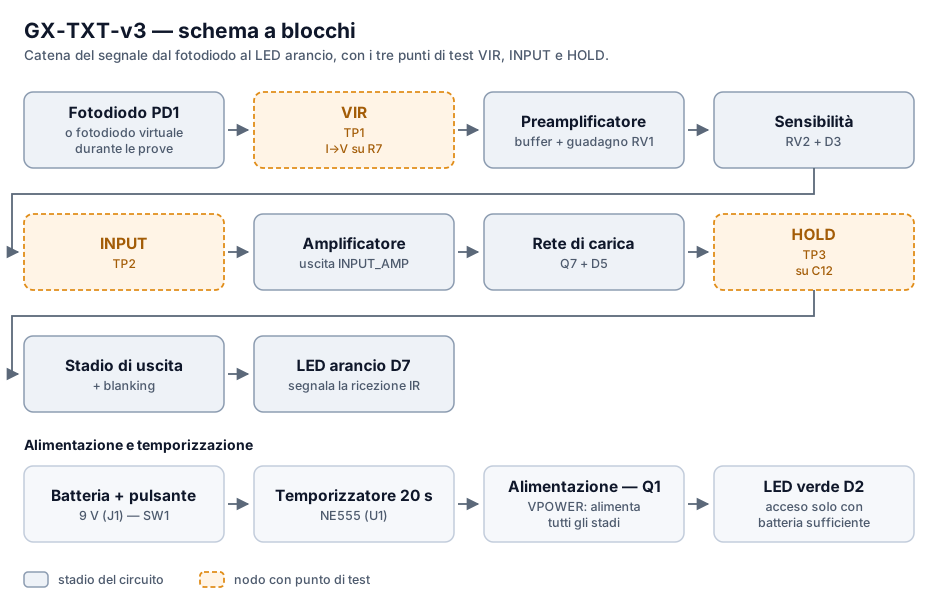
The IR Remote Control Tester is a small instrument powered by a standard 9 V battery, designed to quickly check whether an infrared remote control is working and, above all, to allow qualitative comparisons between different remote controls.
Unlike common integrated IR receivers, which demodulate a fixed carrier frequency, here the signal is taken directly from a photodiode and amplified. The instrument therefore responds to any remote control, regardless of carrier frequency or protocol.
The circuit has two separate adjustments: input-stage gain and sensitivity.
The idea is that, once the circuit has been built, the gain trimmer is adjusted during calibration so that a remote control with a reasonable output power, placed at a similarly reasonable distance, produces the correct response with the sensitivity control set approximately halfway through its range.
From that point on, the gain can remain fixed. During normal use, the sensitivity control is adjusted instead, allowing both the response of different remote controls to be compared and the behavior of the visual indication to be changed.
The IR Remote Control Tester uses two LEDs:
- a green LED, indicating that the instrument is powered on;
- an orange LED, indicating reception of the infrared signal.
The orange LED does not simply follow the IR carrier. The circuit keeps the indication active for a certain interval after the signal ends; depending on the sensitivity setting, this can produce either a brief flash or a more persistent illumination.
The instrument is switched on by a pushbutton. Pressing it powers the circuit for approximately 20 seconds, after which the IR Remote Control Tester switches off automatically. This eliminates the need to remember to turn it off and prevents unnecessary battery drain.
Finally, a simple Zener circuit monitors the battery voltage: below a certain threshold, the green LED does not light, preventing operation with an excessively discharged battery from being mistaken for normal behavior. The threshold still requires a voltage well above 8 V.
The entire circuit was designed to keep the overall size as small as possible, so that it can be installed in a small enclosure and used as a simple bench or portable instrument.
I am starting with v3 simply because I was not yet running the blog when I built the earlier versions. The V1 is still on the bench, however, and I will use it as a reference for comparison in upcoming posts.
Circuit schematic
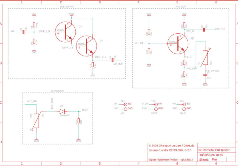
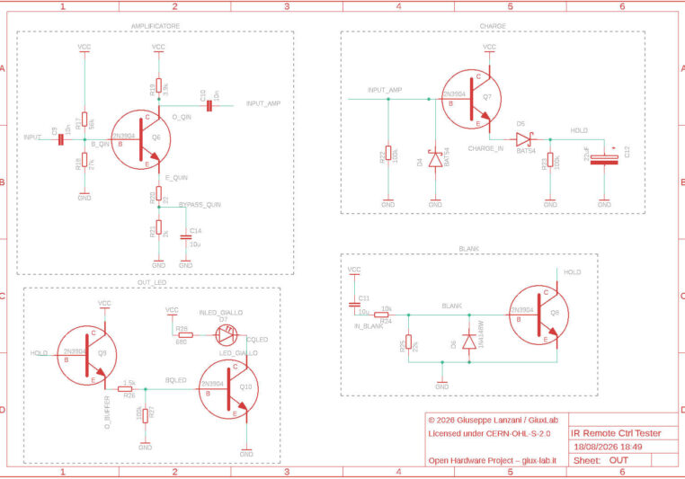
Below are the circuit schematic sheets for the GX-TXT-v3 version, created with Autodesk Fusion.
Here I will not go into the details of the design and simulation of each individual stage; instead, where necessary, I will refer to the simulation results during the subsequent experimental tests.
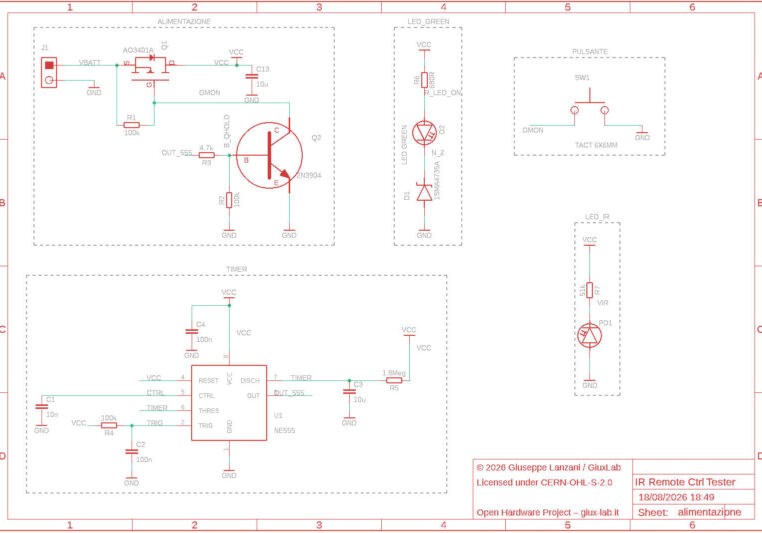 GX-TXT-v3 – Tavola 1: alimentazione, temporizzazione dell’accensione, pulsante e segnalazioni.
Bill of materials
The following bill of materials refers to the GX-TXT-v3 version of the schematic shown above. The listed packages are those used in the Autodesk Fusion project.
| References | Qty. | Package | Value / component |
|---|---|---|---|
| C1, C5, C6, C8, C9, C10 | 6 | C0805 | 10n |
| C2, C4 | 2 | C0805 | 100n |
| C3, C7, C11, C13, C14 | 5 | C1206 | 10u |
| C12 | 1 | TANT_CASE_A_3216_2P_SMD | 22uF |
| D1 | 1 | SMA_DO214AC_2P_SMD | 1SMA4735A |
| D2 | 1 | LED_THT_D5.0MM_P2.54MM | LED GREEN |
| D3, D6 | 2 | SOD123_2P_SMD | 1N4148W |
| D4, D5 | 2 | SOT23_3P_SMD | BAT54 |
| D7 | 1 | LED_THT_D5.0MM_P2.54MM | LED_GIALLO |
| J1 | 1 | JST_XH_1X02_P2.50MM_THT_TOP | |
| PD1 | 1 | LED_THT_D3.0MM_P2.54MM | PD333-3C-H0-L2 |
| Q1 | 1 | SOT23_3P_SMD | AO3401A |
| Q2, Q3, Q4, Q5, Q6, Q7, Q8, Q9, Q10 | 9 | SOT23_3P_SMD | 2N3904 |
| R1, R2, R4, R16, R22, R23, R27 | 7 | R0805 | 100k |
| R3 | 1 | R0805 | 4.7k |
| R5 | 1 | R0805 | 1.8Meg |
| R6 | 1 | R0805 | 680R |
| R7 | 1 | R0805 | 51k |
| R8 | 1 | R0805 | 1Meg |
| R9 | 1 | R0805 | 470k |
| R10, R26 | 2 | R0805 | 1.5k |
| R11, R17 | 2 | R0805 | 56k |
| R12, R18 | 2 | R0805 | 27k |
| R13 | 1 | R0805 | 390 |
| R14 | 1 | R0805 | 1.6k |
| R15, R19 | 2 | R0805 | 3.9k |
| R20 | 1 | R0805 | 22 |
| R21 | 1 | R0805 | 2k |
| R24 | 1 | R0805 | 10k |
| R25 | 1 | R0805 | 22k |
| R28 | 1 | R0805 | 680 |
| RV1 | 1 | RM065_THT_TOP_3P | 1k |
| RV2 | 1 | RM065_THT_TOP_3P | 10k |
| SW1 | 1 | TACT_SWITCH_6X6MM_4P_THT | TACT 6X6MM |
| TP1 | 1 | TESTPOINT_LOOP_PAIR_THT | VIR |
| TP2 | 1 | TESTPOINT_LOOP_PAIR_THT | INPUT |
| TP3 | 1 | TESTPOINT_LOOP_PAIR_THT | HOLD |
| U1 | 1 | SOIC-8_150MIL_P1.27_HAND | NE555 |
PCB and plane management
The following images show the GX-TXT-v3 layout viewed from the top side, respectively with the copper polygons displayed and without fill, making the track routing easier to read as well.
The PCB includes a ground plane and a VPOWER power area. The latter was deliberately excluded from the region around VIR, namely the part of the circuit directly connected to the photodiode and characterized by high impedances.
In this area, a power plane located close to the signal traces could have increased noise coupling into the input. I therefore preferred to avoid VPOWER and use the GND plane instead, adding numerous stitching vias to connect the ground areas on the two sides of the PCB.
The concentration of vias visible around the photodiode and the VIR node is therefore intentional: the goal is to create a ground region that is as continuous as possible around the highest-impedance part of the circuit and to reduce coupling from the power lines and the rest of the board.
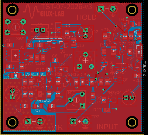 GX-TXT-v3 – Vista top con i poligoni di rame riempiti. Nella zona VIR è stato evitato il piano VPOWER e utilizzata una zona di massa con numerose via di stitching.
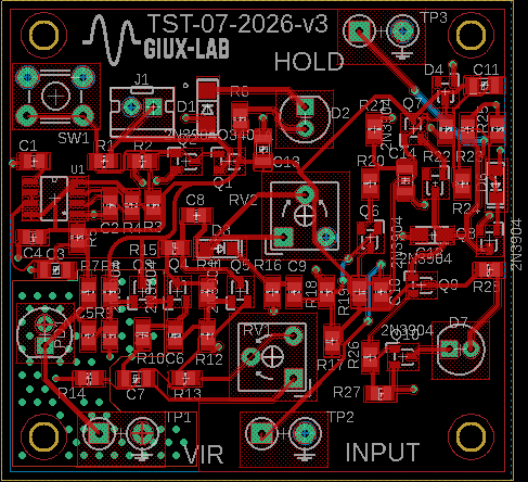
Test pads
The PCB provides three dedicated test points for the VIR, INPUT, and HOLD nodes, highlighted in orange in the block diagram, so that the behavior of the circuit at its main points can be easily observed with an oscilloscope.
VIR is the node directly associated with infrared signal reception. The current generated by the photodiode is converted into a voltage variation mainly through R7; this is therefore the first useful point for observing the signal produced by the photodiode, or the signal generated by the virtual photodiode used during testing.
INPUT is the signal available after the sensitivity adjustment and diode D3. From this node, the signal is sent to the following amplifier stage, which generates INPUT_AMP and then drives the charging network of the HOLD node.
HOLD is the voltage present across capacitor C12. The amplified signal drives Q7 and, through D5, charges this capacitor; the resulting voltage remains present even after the IR signal ends and is used by the output section to keep the orange LED on for a certain period of time.
The three test points therefore make it possible to follow the signal at three distinct stages of the circuit: IR signal reception, processing after sensitivity adjustment, and LED hold voltage.
PCB assembly
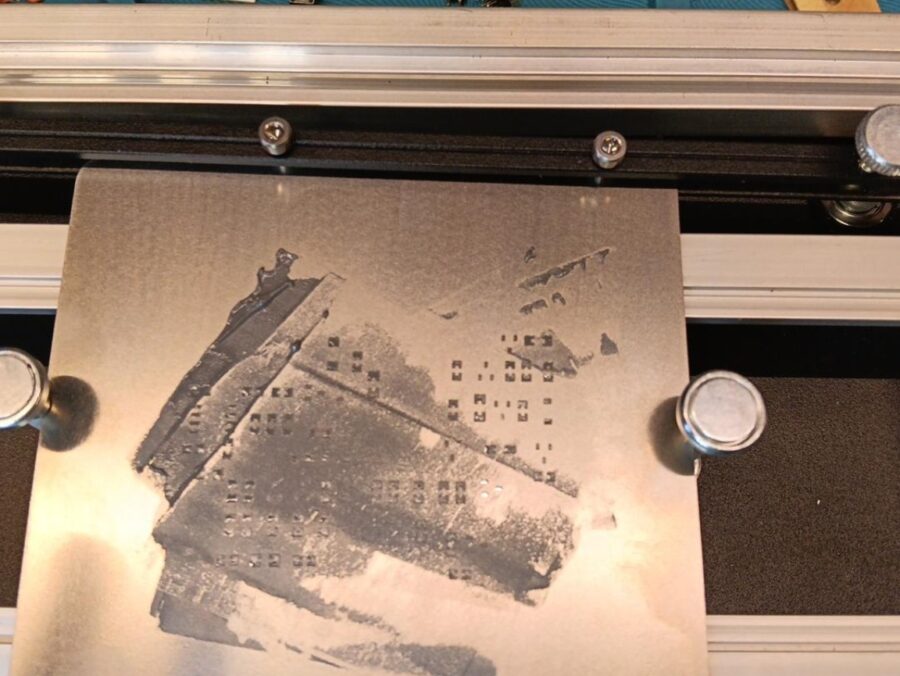
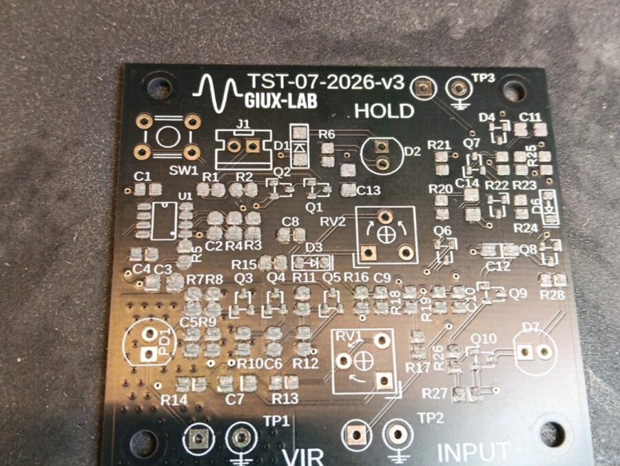
To assemble the GX-TXT-v3, I used the stencil to apply solder paste to the SMD pads.
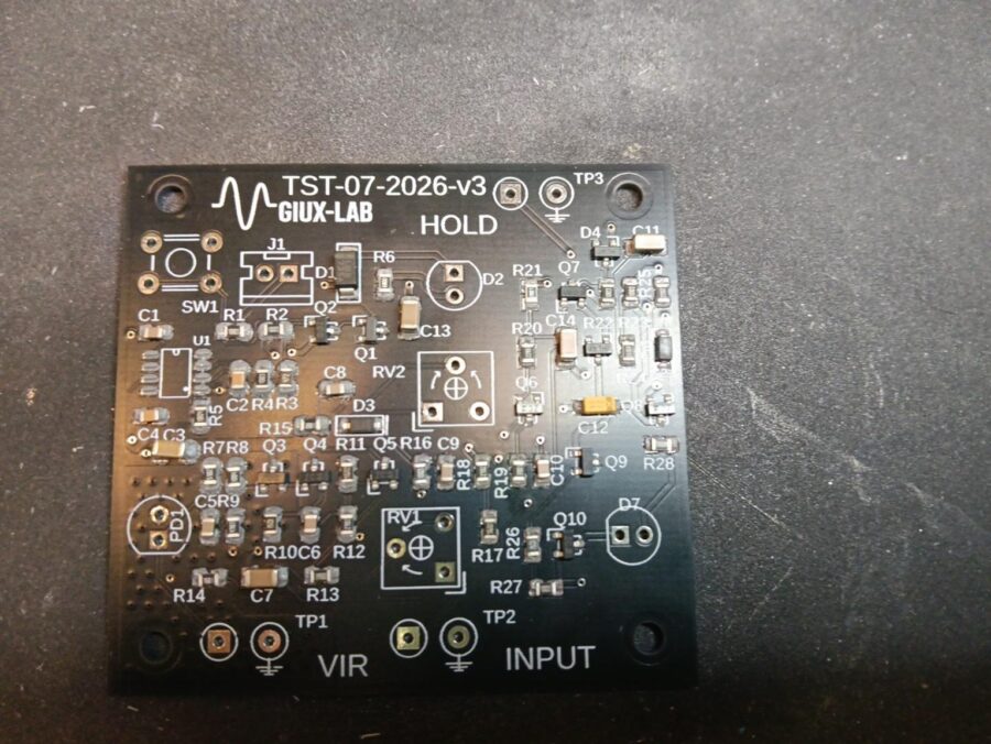
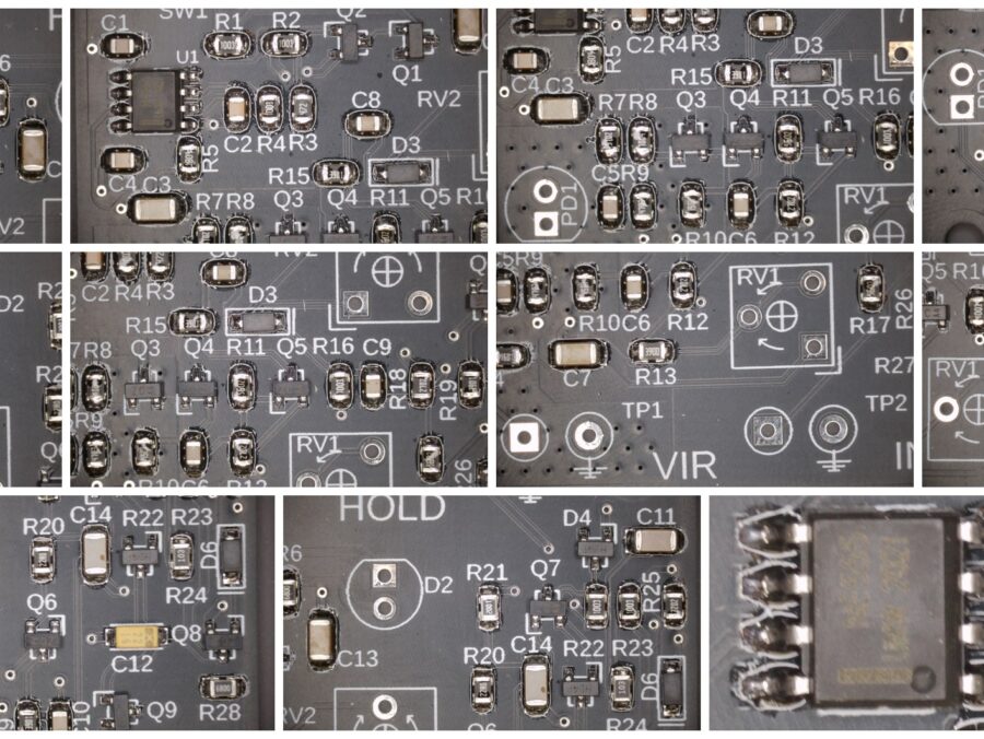
I then placed the SMD components and performed the reflow process. The result after reflow was good, and inspection of the solder joints did not reveal any particular problems.
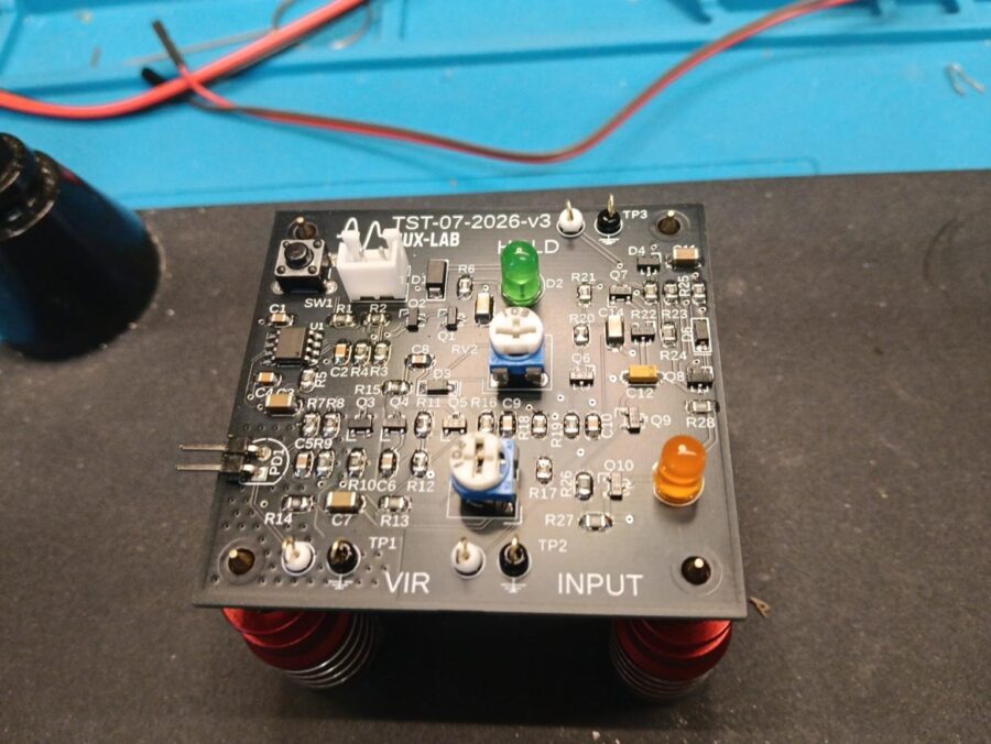
Finally, I completed the board by soldering the through-hole components, and this time the pushbutton footprint is correct, unlike on the previous PCB (v1).
The following gallery shows the main assembly stages, from stencil preparation to the completed GX-TXT-v3, ready for characterization.
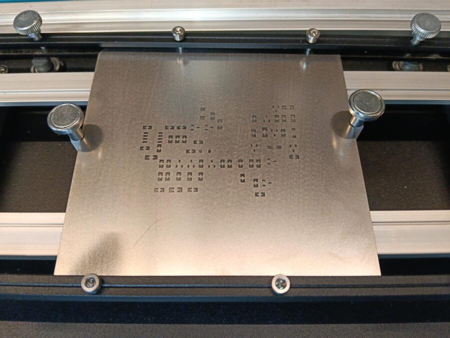 Stencil della GX-TXT-v3 posizionato sulla stampante prima della stesura della pasta.
Next step: V3 characterization
At this point, the GX-TXT-v3 is assembled and ready for measurements.
In the next post, I will start with the DC bias of the various stages, comparing the measured values with the expected ones and checking whether I introduced any errors in the schematic or PCB when moving to the new revision.
I will also compare it with the V1, which is still available and working on the bench, highlighting the main differences between the two versions and checking how much they affect the actual behavior of the circuit.
Only after this initial verification will I move on to the actual dynamic characterization.