

GX-TXT-v3: Virtual Photodiode and Preamplifier Measurements
Starting point
The GX-TXT-v3 is a compact instrument designed to check the operation of infrared remote controls. The circuit detects the received signal, amplifies its useful component, and drives an indicator LED, with adjustable sensitivity and automatic shutoff after a few seconds to reduce battery consumption.
In this series of articles I am following the construction and characterization of the circuit step by step, from PCB design to bench measurements.
Here is the first post in the series:
Test equipment used
For the measurements described in this article I mainly used a RIGOL DS1104Z-S Plus, with the 20 MHz bandwidth limit enabled to reduce unnecessary high-frequency noise during these tests.
Oscilloscope measurements were performed with a RIGOL PVP3150 used in 10×. In this configuration, the probe has a nominal input impedance of 10 MΩ and a capacitance of about 10 pF.
As the function generator I used an FE FY6900, used to drive the virtual photodiode with the waveforms required for the various tests.
For DC measurements I mainly used the OWON XDM2041. For some checks and auxiliary measurements I also used a NIMEX NI-4000.
The virtual photodiode
To characterize the circuit repeatably, at least initially I preferred not to use a real photodiode. Instead, I use a small circuit that acts as a virtual photodiode and allows me to generate a controlled current from the signal provided by the function generator.
The circuit is intentionally very simple. The GEN_IN signal drives the base of a 2N3904 through a 1 kΩ resistor; a 1 MΩ resistor keeps the base referenced to ground when no signal is present. The emitter has a 51 kΩ RSENSE resistor, while the collector is connected directly to the VIR node of the IR Remote Control Tester.
In this way, the transistor essentially operates as a current source controlled by the voltage applied to GEN_IN. Within the approximations of the circuit, the current drawn by the collector therefore simulates the current that would be produced by an illuminated real photodiode.
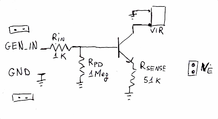
The collector of the 2N3904 is connected directly to the VIR node of the GX-TXT-v3. In the IR Remote Control Tester, this node is pulled toward the supply, about 9 V, through the 51 kΩ R7 resistor.
With no current flowing, VIR is therefore practically at the supply voltage. When the virtual photodiode transistor conducts, it draws current from the node and a voltage drop appears across R7. As a first approximation, we can therefore write:
VIR ≈ VCC – IC · R7
Limitations of the virtual photodiode
This circuit is not intended to be a complete model of a real photodiode. Its main purpose is to provide a controllable and repeatable current with which to verify the response of the GX-TXT-v3 input chain.
A real photodiode also has junction capacitance, as well as dark current, parasitic resistance, and its own noise characteristics. Photodiode capacitance can become particularly important in AC measurements because, together with the impedance of the circuit to which it is connected, it affects the signal shape and frequency response.
This capacitance is intentionally not reproduced in the virtual photodiode: at the 2N3904 collector there remain only the transistor’s own capacitance, on the order of a few pF, and the parasitic capacitances introduced by the construction, connections, and measuring instruments.
The two systems are not equivalent in terms of noise either. The transistor naturally has its own noise, but the circuit does not exactly reproduce the noise associated with an illuminated real photodiode.
Current limit and headroom
There is naturally a limit to the current that the virtual photodiode can simulate. For the 2N3904 to continue operating correctly, the collector voltage must remain sufficiently higher than the emitter voltage; if VIR dropped too low, the transistor would enter saturation and the relationship between control voltage and current would no longer be valid.
At the highest point used in this test, about 38 µA, I measure about 1.95 V at the emitter. The same current produces a drop of about 1.94 V across the 51 kΩ R7 resistor of the GX-TXT-v3: starting from about 9 V, VIR therefore remains around 7 V. The transistor still has several volts between collector and emitter and is therefore far from saturation.
Neglecting the small difference between collector and emitter current, with both R7 and RSENSE equal to 51 kΩ, the limit imposed by saturation is roughly in the 80–85 µA range with a 9 V supply. The values used in these tests therefore remain well below this limit.
Virtual photodiode implementation
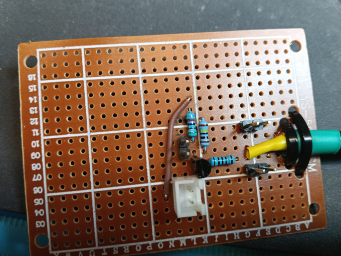
I built the virtual photodiode on a small prototyping board, keeping the ground paths on the two sides of the circuit separate as far as practical.
The function generator is connected to GEN_IN through a coaxial cable. The shield is soldered directly to the board GND close to the generator input, keeping the drive-signal return path short.
On the VIR side, I instead placed the connector ground contact directly close to the lower end of RSENSE. In this case, the current I want to simulate enters the circuit from the VIR node, flows through the collector and emitter of the 2N3904, and returns to ground through RSENSE. The base current is only a small fraction of the total current: by placing the return to the IR Remote Control Tester here, I keep the main-current path as short as possible, avoiding unnecessarily routing it through other areas of the board ground.
For the connection to the GX-TXT-v3, I also replaced the previous pin headers with JST-XH connectors, both on the virtual photodiode and at the position originally intended for the board photodiode. The two circuits are connected by a very short cable made from a lightly twisted pair. Compared with standard Dupont jumpers, this provides a mechanically more stable and repeatable connection during measurements while keeping the VIR connection very short.
Generated-current characterization
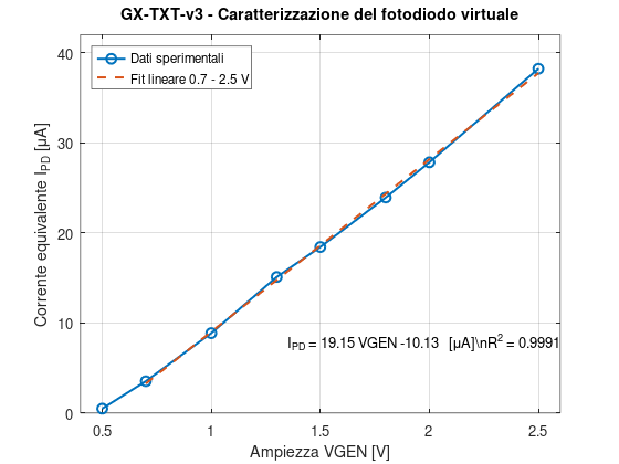
Before using the virtual photodiode for measurements on the GX-TXT-v3, I experimentally measured the generated current for several VGEN values.
For this test I used an approximately 38 kHz square wave with a duty cycle close to 50%. The generator has a 50 Ω output but drives a high-impedance input; the amplitude shown in the table is the value actually measured at GEN_IN with the yellow oscilloscope channel.
During the measurement I used two oscilloscope channels: the yellow channel monitors GEN_IN, while the blue channel measures the voltage at the emitter of the 2N3904, directly across RSENSE.
As a first approximation, the generated current can also be interpreted using the relationship:
I ≈ (VGEN – VBE) / RSENSE
This is only an approximate relationship, because VBE is not constant, and the 1 kΩ resistor in series with the base also develops a small voltage drop due to base current.
To determine the values reported in the table, I therefore used the measured VE voltage directly, from which the emitter current can be calculated. The current actually drawn from the VIR node is the collector current and differs from the emitter current only by the transistor base current; for this characterization I therefore consider IC approximately equal to IE.
IPD ≈ IE = VE / RSENSE = VE / 51 kΩ
| VGEN amplitude | Measured VE | Equivalent current |
|---|---|---|
| 0.5 V | 24.60 mV | 0.5 µA |
| 0.7 V | 180 mV | 3.5 µA |
| 1.0 V | 452 mV | 9 µA |
| 1.3 V | 770 mV | 15 µA |
| 1.5 V | 940 mV | 18 µA |
| 1.8 V | 1.220 V | 24 µA |
| 2.0 V | 1.420 V | 28 µA |
| 2.5 V | 1.950 V | 38 µA |
The following waveforms show the characterization of the virtual photodiode for several VGEN values. The yellow channel shows GEN_IN, while the blue channel shows the voltage at the emitter of the 2N3904 and therefore, through RSENSE, the waveform of the generated current.
As VGEN is progressively increased, the emitter voltage and therefore the equivalent virtual-photodiode current increase. The images correspond to the same points used to build the current table.
 VGEN = 0,5 V. In giallo il segnale GEN_IN e in azzurro la tensione sull’emettitore del 2N3904, misurata ai capi di RSENSE. VE = 24,6 mV, corrispondente a circa 0,5 µA.


After this series of measurements, I soldered a jumper across the power button to keep the IR Remote Control Tester continuously powered during the following tests. During measurements, the timer could otherwise switch the circuit off and force me to reactivate it.
AC characterization of the input and preamplifier
Signal measurement at the VIR node
The first point in the chain I chose to observe is VIR, the node to which the virtual photodiode collector is connected and, during normal instrument operation, the real photodiode.
VIR is connected to the supply, about 9 V, through the 51 kΩ R7 resistor. With no current flowing, the node therefore remains close to the supply voltage; when the virtual photodiode conducts, the current drawn from the node produces a drop across R7 and the VIR voltage decreases.
Before comparing the simulation with the real measurement, I repeated the LTspice simulation using the complete circuit and also included the oscilloscope-probe loading. The measurement is performed with a RIGOL PVP3150 in 10× configuration, which at the probe tip has a nominal impedance of about 10 MΩ in parallel with about 10 pF. I therefore added a 10 MΩ resistor and a 10 pF capacitor between VIR and ground in the simulation.
The resistive component of the probe has a very small effect when compared directly with the 51 kΩ R7 resistor, but this does not mean that the measurement can be considered completely non-invasive. The following buffer stage is also connected to the VIR node through the 10 nF coupling capacitor.
At the frequency used for these tests, about 38 kHz, the reactance of the 10 nF capacitor is about 420 Ω and is therefore very small compared with the resistances in the buffer bias network. From an AC point of view, the VIR node is therefore also affected by the impedance of the following stage, whose divider includes 1.8 MΩ and 470 kΩ.
At this point, the probe capacitance becomes more important. A capacitance of about 10 pF has, at 38 kHz, a reactance of about 420 kΩ, comparable to the impedance of the buffer input network. At the higher harmonics that form the square-wave edges, its reactance decreases further, so the effect of the probe can become visible especially in the shape of the transitions.
For this reason, when comparing the simulation with the real waveform, I explicitly included the probe model as well. In this way, the simulation represents not only the ideal circuit, but more precisely the circuit under the conditions in which it is actually observed on the bench.
To maintain consistency with the simulation, I set the generator to an amplitude of VGEN = 1.58 V. Under these conditions, I measure about 1.02 V, which through RSENSE of 51 kΩ corresponds to a current of about 20 µA.
At this point I directly compared the simulated VIR node with the one measured on the real board, keeping the equivalent photodiode current at about 20 µA.
The following two images show first the LTspice simulation result, including probe loading, and then the waveform acquired on the bench under the same operating conditions.
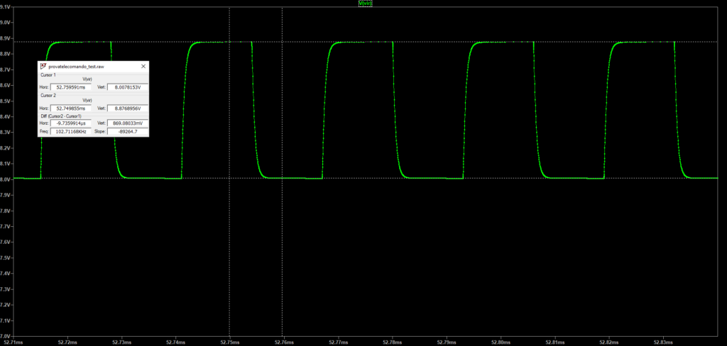

The agreement is very close. In simulation, the voltage change at the VIR node is about 869 mV, while on the hardware I measure about 860 mV. The difference is therefore only 9 mV, about 1%: simulation and measurement agree within the uncertainty due to component tolerances.
The transition shape is also qualitatively very similar. The real signal, like the simulated signal including probe loading, has rounded edges rather than a perfectly rectangular transition. For this first measurement, the VIR-node behavior is therefore very close to that predicted by the model.
Effect of the gain adjustment on the QPRE preamplifier
After verifying the behavior of the VIR node, I moved on to the first actual amplification stage of the GX-TXT-v3, observing the signal at the collector of QPRE, node QPRE_C in the simulation.
In this test I kept the virtual-photodiode drive unchanged, with an equivalent current of about 20 µA, and progressively changed the POT_GAIN adjustment. The purpose is to verify how much the signal amplitude at the QPRE collector changes and to compare the behavior of the real circuit with that predicted by LTspice.
I preferred to perform the measurement at the collector rather than at the transistor base. The signal swing is much larger at the collector and therefore easier to read, whereas a measurement at the input nodes would show smaller variations and would introduce loading in the most sensitive part of the stage.
For each trimmer position, I measured the peak-to-peak swing at QPRE_C with the oscilloscope. I also recorded the voltage indicated by the OWON XDM2041 bench multimeter in LOW acquisition mode. This value is reported only as a reference: since the signal is periodic but not perfectly symmetrical, and since I do not know in detail how the instrument processes the signal in this mode, I will not use it for a quantitative comparison with the simulation.
In this simulation I did not add the 10 MΩ // 10 pF probe model previously used at the VIR node. QPRE_C is a significantly lower-impedance node, so the loading introduced by the 10× probe is much less significant.
The actual measured trimmer settings were 0 Ω, 249.0 Ω, 498.2 Ω, 749.8 Ω, and 960.8 Ω. I used the same respective values in the simulation.
POT_GAIN = 0 Ω
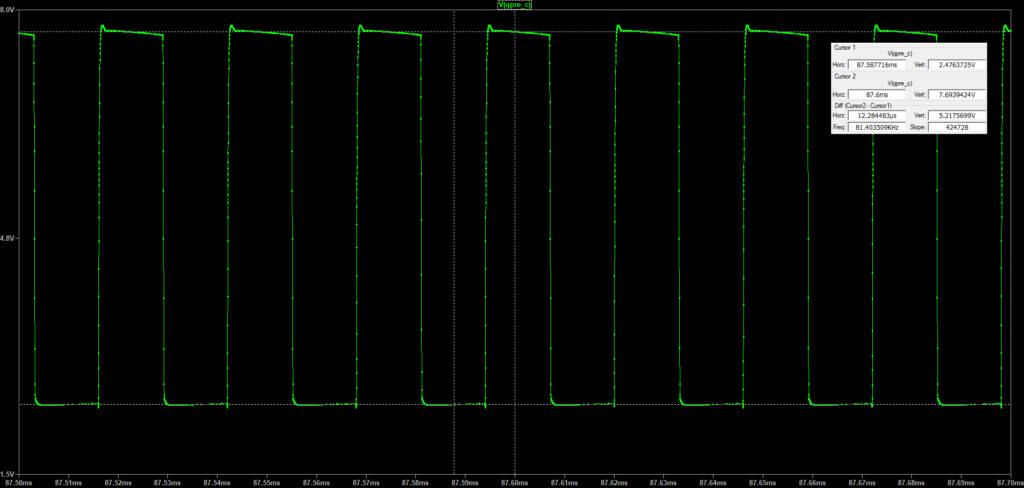
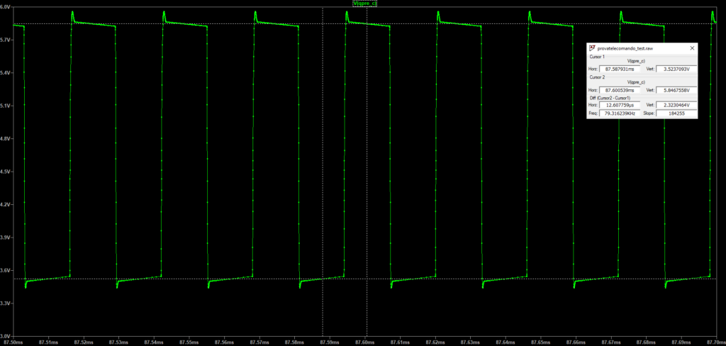
With POT_GAIN set to 0 Ω, the stage has maximum gain. On the real circuit I measure about 5.02 Vpp at the QPRE collector, while the simulation predicts about 5.22 Vpp. The DC reading provided by the OWON is 5.0139 V.

POT_GAIN ≈ 250 Ω
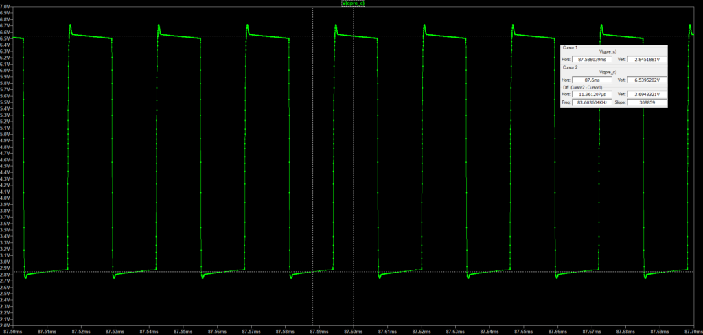
Setting POT_GAIN to 249.0 Ω, the measured swing decreases to about 3.64 Vpp. The simulation performed with the same POT_GAIN value gives about 3.69 Vpp. The OWON reading is 4.7247 V.

POT_GAIN ≈ 500 Ω
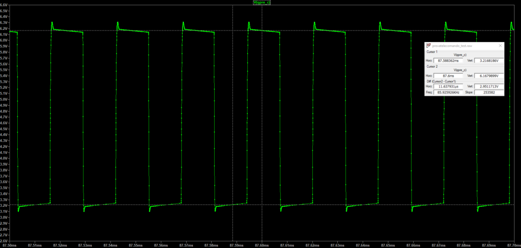
With POT_GAIN equal to 498.2 Ω I obtain about 2.82 Vpp on the real circuit. Under the same conditions, the simulation returns about 2.95 Vpp. The OWON reading is 4.711 V.

POT_GAIN ≈ 750 Ω
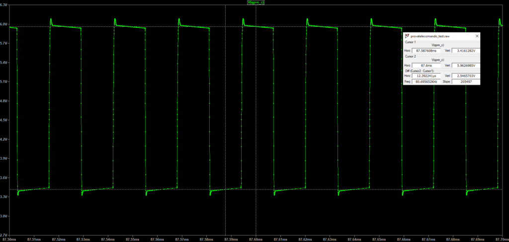
With POT_GAIN equal to 749.8 Ω the real swing decreases to about 2.45 Vpp, while the simulation gives about 2.55 Vpp. The OWON reading is 4.722 V.

POT_GAIN ≈ 1 kΩ
In the final measurement, POT_GAIN is 960.8 Ω. On the real circuit I measure about 2.26 Vpp, while the simulation performed with the same value gives about 2.32 Vpp. The OWON reading is 4.709 V.

Summary of preamplifier measurements
The following table summarizes the results obtained at the QPRE_C node for the five POT_GAIN settings used during the test. For each point, I report the peak-to-peak swing measured on the hardware and that obtained in LTspice under the same conditions.
I also report the voltage read by the OWON XDM2041 bench multimeter. The measurement was performed using the instrument’s LOW acquisition mode and, since this is a varying waveform, I do not consider it a sufficiently well-defined DC operating-point measurement for quantitative comparison with the simulation. It remains useful as an experimental reference.
| POT_GAIN | OWON reading (LOW) | Measured QPRE_C | QPRE_C LTspice |
|---|---|---|---|
| 0 Ω | 5.0139 V | 5.020 Vpp | 5.218 Vpp |
| 249.0 Ω | 4.7247 V | 3.640 Vpp | 3.694 Vpp |
| 498.2 Ω | 4.711 V | 2.820 Vpp | 2.951 Vpp |
| 749.8 Ω | 4.722 V | 2.450 Vpp | 2.547 Vpp |
| 960.8 Ω | 4.709 V | 2.260 Vpp | 2.323 Vpp |
Amplification ratio between VIR and QPRE_C
The collected data can also be used to determine the ratio between the swing at the QPRE collector and the swing previously measured at the VIR node.
It is important to note that this value does not represent the gain of the QPRE transistor alone. Between VIR and QPRE there are in fact the coupling capacitor, the Darlington buffer formed by QBUF1 and QBUF2, and the following coupling capacitor toward the preamplifier. The calculated value therefore describes the overall amplification ratio of the chain between VIR and QPRE_C under the conditions used for this test.
AVIR→QPRE_C = Vpp(QPRE_C) / Vpp(VIR)
For the real circuit I use the previously measured swing at the VIR node, about 860 mVpp. For the simulation I instead use the corresponding LTspice value of about 869 mVpp. In this way, the ratio is calculated separately from the real and simulated data.
Areal = Vpp(QPRE_C)real / 0.860 V
Asim = Vpp(QPRE_C)sim / 0.869 V
| POT_GAIN | Measured ratio | LTspice ratio |
|---|---|---|
| 0 Ω | 5.84 | 6.00 |
| 249.0 Ω | 4.23 | 4.25 |
| 498.2 Ω | 3.28 | 3.40 |
| 749.8 Ω | 2.85 | 2.93 |
| 960.8 Ω | 2.63 | 2.67 |
To make the comparison more immediate, I plotted these values with the resistance set by POT_GAIN on the horizontal axis and the VIR → QPRE_C amplification ratio on the vertical axis. The graph includes both the experimental data and the values obtained from the LTspice simulation.
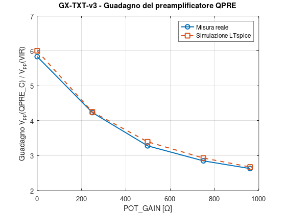
The measured trend follows the simulation very closely. As POT_GAIN is increased from 0 Ω toward the end of its range, the overall VIR → QPRE_C amplification ratio changes from about 5.84 to 2.63 on the real circuit, while LTspice predicts a change from about 6.00 to 2.67.
The adjustment therefore produces the expected effect: increasing POT_GAIN progressively reduces the amplification of the AC component, with a very similar trend in the real circuit and the model.
A visible difference remains in the shape of the collector voltage. In the simulation, the level during each half-cycle has a more noticeable slope, while on the real hardware the waveform is flatter. At this stage I therefore consider the agreement in amplitude and gain trend to be very good, while leaving the difference in the detailed signal shape open for further investigation.
Conclusions
The measurements experimentally verify the behavior of the first part of the GX-TXT-v3 signal-processing chain. The virtual photodiode makes it possible to apply a known and repeatable current to the VIR node, enabling a direct comparison between the real circuit and the simulation.
At the VIR node, the measured change was very close to that predicted by LTspice. At the QPRE collector, the POT_GAIN adjustment also produces the expected effect: as the resistance increases, the signal amplitude progressively decreases, with good agreement between measured and simulated values.
Under the test conditions, the overall amplification ratio between VIR and QPRE_C changes from about 5.84 with POT_GAIN at 0 Ω to about 2.63 with POT_GAIN at 960.8 Ω. The simulation gives corresponding values of about 6.00 and 2.67.
It is worth clarifying the role of simulation in these tests. The objective is not to obtain exact numerical agreement between LTspice and the bench, but to characterize the behavior of the real circuit. The simulation therefore serves as a check: if measurement and model agree within a few percentage points, I can consider the circuit to be behaving as expected, with no major errors either in assembly or in the way I am measuring it.
In these measurements, the difference between hardware and simulation consistently remains within about 4.5%, with the measured amplitude always slightly lower than predicted. This difference is compatible with component tolerances and model approximations and does not change any of the conclusions. The same applies to the different slope observed during the half-cycles: it remains a point for further investigation, but it does not affect the gain characterization, which was the objective of these measurements. The measured values therefore remain the reference values for the board.
With this test, I therefore consider the gain adjustment of the first part of the chain experimentally characterized. The next step will be to study the sensitivity adjustment and trigger threshold, which involves a different part of the circuit and requires a dedicated set of measurements.