

GX-TXT-v3: IR Remote Control Tester – DC Bias and Timer Verification
Today, as anticipated, I checked the DC operating point, comparing the voltages measured on the PCB with those predicted by the simulation.
I started from here:
To make the measurements easier to read, I used more memorable names for the main transistors, also reflecting their role in the circuit, instead of constantly referring only to designators Q3, Q4, Q5, and so on.
At this stage I did not, of course, measure the sections of the circuit that operate only during the transient generated when an IR signal is received. These will be analyzed later during the dynamic characterization.
| Name used | Reference | Function |
|---|---|---|
| QBUF1 | Q3 | First transistor of the Darlington buffer pair |
| QBUF2 | Q4 | Second transistor of the Darlington buffer pair |
| QPRE | Q5 | Preamplifier |
| QIN | Q6 | Following amplifier stage |
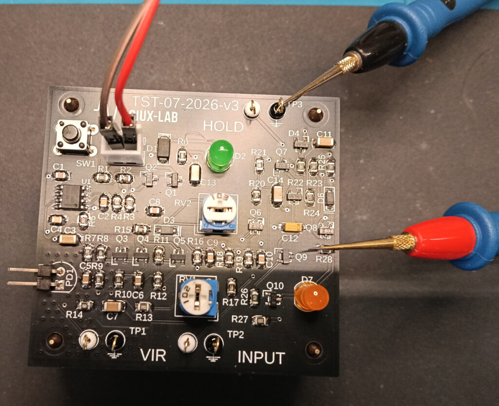
Comparison between simulation and DC measurements
The following table compares the operating-point values obtained in simulation with those measured on the GX-TXT-v3. The deviation is calculated as the difference between the measured value and the simulated value.
| Node | Simulation | Measured | Δ | Deviation |
|---|---|---|---|---|
| VBAT | 9.000 V | 9.010 V | +10 mV | +0.11% |
| VCC | 8.999 V | 8.982 V | -17 mV | -0.19% |
| QBUF1 – B | 2.874 V | 2.773 V | -101 mV | -3.51% |
| QBUF1 – E | 2.366 V | 2.392 V | +26 mV | +1.10% |
| QBUF2 – E | 1.709 V | 1.718 V | +9 mV | +0.53% |
| QPRE – B | 2.861 V | 2.834 V | -27 mV | -0.94% |
| QPRE – E | 2.204 V | 2.193 V | -11 mV | -0.50% |
| PREGAIN | 1.772 V | 1.764 V | -8 mV | -0.45% |
| QPRE_C | 4.694 V | 4.733 V | +39 mV | +0.83% |
| QIN – B | 2.862 V | 2.808 V | -54 mV | -1.89% |
| QIN – C | 4.759 V | 4.795 V | +36 mV | +0.76% |
| QIN – E | 2.205 V | 2.181 V | -24 mV | -1.09% |
Overall, the measured values are very close to those predicted by the simulation. The largest deviation is observed at the base of QBUF1, while at the other nodes the differences generally remain around 1-2% or less.
However, the QBUF1 base node deserves a clarification.
The base of QBUF1 is biased by a high-impedance divider, R8 = 1 MΩ and R9 = 470 kΩ, which presents an equivalent resistance of about 320 kΩ at the node. This is the only measured point where the source impedance is not negligible compared with the input impedance of a multimeter.
I therefore repeated the simulation by adding a 10 MΩ resistor from that node to ground to represent the load introduced by the instrument during measurement. Under these conditions LTspice gives 2.785 V, compared with the 2.773 V measured on the PCB, leaving a residual difference of 12 mV.
The deviation observed at the base of QBUF1 therefore appears to be mainly due to multimeter loading rather than to a real difference between the circuit and the simulation. To state this with certainty, however, the actual input impedance of the Owon XDM2041 on the range used should be checked; I have not yet verified it in the manual. I therefore leave this point open for a later check.
At all the other measured nodes the source impedance is only a few kΩ, so the loading effect of the instrument is negligible and this issue does not arise.
Power supply and battery monitoring
One point to keep in mind when comparing the simulation with the real circuit is that the GX-TXT-v3 does not use a regulated power supply. During these tests the board was powered directly from the bench power supply, set to around 9 V.
A small shift in the bias points relative to the simulated values is therefore normal. This behavior is also consistent with the intended use: the IR Remote Control Tester is designed to operate from a 9 V battery, whose voltage inevitably changes as it discharges. The circuit must therefore maintain sufficiently stable operating points even with a supply voltage that is not perfectly constant.
Battery-voltage monitoring and green LED
I deliberately added a D1 Zener diode. The purpose is to prevent the LED from continuing to light normally when the battery voltage has become too low.
I also compared simulation and real measurements for this part of the circuit. The voltage across the Zener is 6.21 V in LTspice and 6.26 V on the real circuit.
At the upper node of the green LED, that is, after resistor R6, the simulation gives 8.249 V, while on the PCB I measured 8.556 V. The measured voltage across the LED is therefore approximately:
VLED = 8.556 V – 6.26 V = 2.296 V
Since R6 = 680 Ω and it is a 1%-tolerance resistor, we can also estimate the current through the green LED quite accurately. With the measured VCC equal to 8.982 V, the voltage drop across R6 is:
VR6 = 8.982 V – 8.556 V = 0.426 V
and therefore:
ILED = 0.426 V / 680 Ω ≈ 0.626 mA
Considering only the 1% tolerance of R6, the current is approximately between 0.620 mA and 0.633 mA.
| Quantity | LTspice | Measured |
|---|---|---|
| VCC | 8.999 V | 8.982 V |
| D1 Zener voltage | 6.21 V | 6.26 V |
| Upper green-LED node | 8.249 V | 8.556 V |
| Voltage drop across green LED | 2.039 V | 2.296 V |
| Green LED current | about 1.10 mA | about 0.626 mA |
The actual LED current is therefore lower than predicted by the simulation, while the Zener voltage remains practically unchanged. The difference is mainly due to the different operating point of the real LED compared with the model used in LTspice.
This is naturally not a hard threshold like the one that would be obtained using a comparator. The LED brightness decreases progressively as the battery voltage falls, according to the actual characteristics of the Zener diode and the LED itself.
The purpose of the circuit is simply to provide a practical indication of battery condition. In the tests performed, with a VBAT of about 8.3 V, the green LED, although a very small current may still flow through it, appears to my eyes practically invisible. A battery that has reached this level is therefore, in practice, indicated as no longer sufficiently charged for normal use of the instrument.
Current consumption
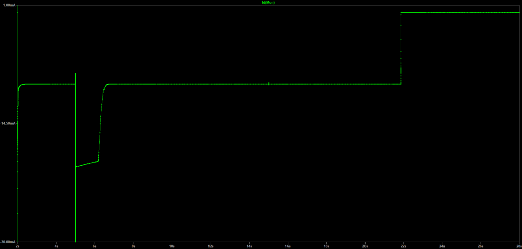
I also measured the current drawn by the board in its different operating states. To do this, I opened the VBAT line and inserted the multimeter in series, using it as an ammeter.
At this stage I had not yet connected either the real photodiode or the virtual photodiode. To turn on the orange LED, I simply touched the pin header connected to the VIR.
VIR is a high-impedance node, and the capacitive coupling introduced by the body is sufficient to generate interference that is amplified by the receiver chain until the orange LED turns on. This is obviously not a functional test of the IR receiver, but simply an easy way to bring the circuit into its maximum-current state.
| Circuit state | Measured current |
|---|---|
| Circuit off | 0.7 mA |
| Circuit on: green LED + DC bias currents | 8.8 mA |
| Circuit on: green LED + active chain + orange LED | 19 mA |
Current consumption therefore increases from about 0.7 mA with the circuit off to about 8.8 mA during normal operation, including the green LED and the bias currents of the various stages. When the chain that turns on the orange LED is also activated, total current consumption rises to about 19 mA.
For current consumption, I also compared the measurements made on the real board with the values predicted by the LTspice simulation. In the graph, the current appears with an inverted sign while it is being drawn; this is simply the convention used by the simulator. The table therefore reports the magnitudes.
| Circuit state | LTspice | Measured |
|---|---|---|
| Circuit off | about 0 mA | 0.7 mA |
| Green LED on + DC bias currents | 9.33 mA | 8.8 mA |
| Green LED + active chain + orange LED on | about 19.7 mA | 19 mA |
In the two operating states, the measured values are therefore reasonably consistent with the simulation. With the green LED on and the stages biased, I measure 8.8 mA compared with 9.33 mA predicted by LTspice; when the orange LED also turns on, total current consumption rises to 19 mA, compared with about 19.7 mA obtained in simulation.
The origin of the approximately 0.7 mA measured with the circuit off remains to be understood, since the simulation predicts practically zero current consumption.
An important check is that, under this condition, with the green LED off and the system inactive, I measured VCC = 0 V. The main part of the circuit is therefore effectively unpowered, and only the power-on control network remains directly connected to VBAT.
The areas still to be checked therefore include the network around MOSFET Q1 and Q2, including its base/pull-down resistor, as well as possible leakage currents in the real components. At present, however, I do not have sufficient evidence to assign the measured 0.7 mA to any one of these paths with certainty.
The value may also be affected by the characteristics of the NIMEX NI-4000 multimeter used for the measurement. I therefore prefer to report it as experimental data without assigning it, for now, to a cause that I have not verified.
Power-on timer verification
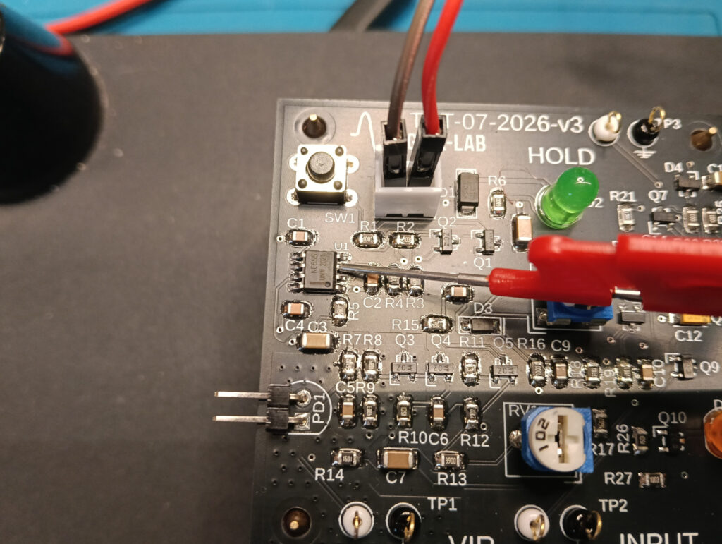
I also checked the duration of the timer that keeps the IR Remote Control Tester powered after the button is pressed.
The timing network uses an NE555 with R = 1.8 MΩ and C = 10 µF. I simply show here the schematic used in the simulation.
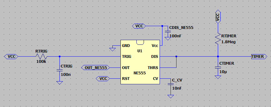
The timer is powered from VCC rather than directly from VBAT. When the circuit switches off, power is therefore also removed from the NE555 and its timing network, returning the system to its initial state.
In the LTspice simulation, I measured an output-pulse duration of 19.84 s, using the cursors; this also essentially matches the nominal value expected from the RC network.
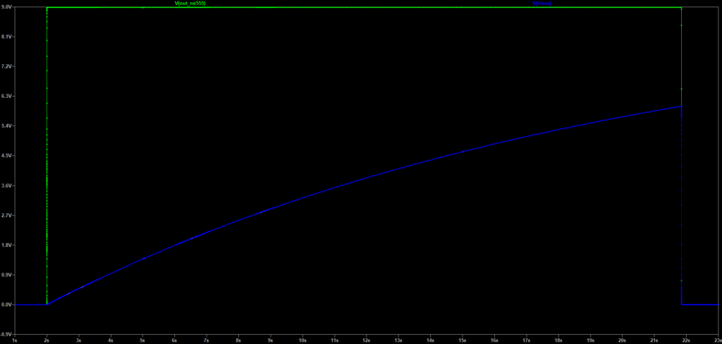
On the real circuit I chose not to measure the TIMER. The timing resistor is 1.8 MΩ, and even a standard 10× probe, with an input resistance on the order of 10 MΩ, would have loaded the RC network significantly enough to alter the very time interval I wanted to measure.
Since I do not have a 100× probe, I therefore measured OUT_NE555: the falling edge of the output still identifies the end of the timing interval accurately without significantly disturbing the RC network.
The acquisition made with the Rigol oscilloscope gives a duration of 20.6 s.

| Method | Duration |
|---|---|
| Nominal R-C value | about 19.8 s |
| LTspice simulation | 19.84 s |
| Actual measurement with Rigol | 20.6 s |
The difference between simulation and the actual measurement is 0.76 s, corresponding to about 3.8%. Considering the tolerances of the real components, particularly the 10 µF capacitor, I therefore consider the measured timing interval fully consistent with the expected value.
Main differences between V1 and V3
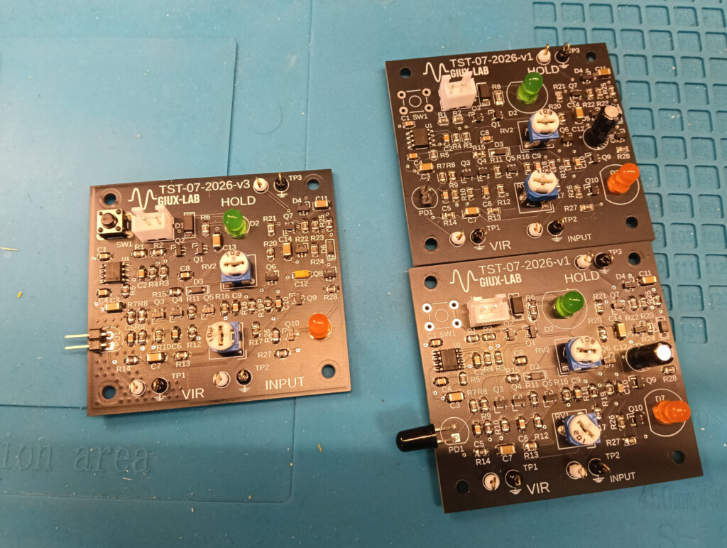
Before moving on to dynamic measurements, it is worth briefly summarizing the main differences between the GX-TXT-v1 and the new GX-TXT-v3.
The first change concerns the power button. In V1 I had made a mistake in the footprint design; the footprint was therefore redesigned and is finally correct in V3.
In V1 I had also fitted some resistor values slightly different from those used in V3, simply because at the time I did not have all the values specified by the design:
- R11 and R17: 51 kΩ in V1, 56 kΩ in V3;
- R9: 464 kΩ in V1, 470 kΩ in V3;
- R7, at the VIR node: 49.9 kΩ in V1, 51 kΩ in V3.
I also replaced C12, which in V1 was a standard electrolytic capacitor, with a tantalum capacitor.
V3 also includes C13, which had been omitted in the first revision. It is not essential to board operation, but an additional ceramic capacitor on the input supply can only help, and I expect it may also contribute to cleaner measurements.
The most obvious PCB change, however, is the introduction of the VPOWER plane, which was absent in V1. I deliberately kept it away from the VIR node and the divider that biases QBUF1, where the impedances are high and therefore more sensitive to unwanted coupling. In that area I preferred to use ground and numerous stitching vias.
V1 nevertheless works well and has already been characterized, so I do not expect major problems from V3.
The old PCBs will also remain useful for some later tests: in particular, I want to use them to compare circuit behavior with different photodiodes.
Instruments used
The instruments used for the measurements described in this post are listed below.
| Instrument | Use | Notes |
|---|---|---|
| Owon XDM2041 bench multimeter | DC voltages: bias points of the various stages, D1 Zener, green LED | 50 V range |
| NIMEX NI-4000 multimeter | Current drawn by the board in the different states, connected in series with the VBAT line | 200 mA range |
| Rigol DS1104Z-S Plus oscilloscope with 10× probe | Timing duration, acquired at the OUT_NE555 node | |
| GVDA bench power supply | Board power supply, set to around 9 V | Instead of the 9 V battery |
Next step: virtual photodiode and transient measurements
At this point, the static behavior of the GX-TXT-v3 is consistent with expectations: the DC bias points agree with the simulation, current consumption is plausible, and the NE555 timing is very close to the expected value.
In the next post I will therefore move on to the part that actually comes into play when an IR signal arrives.
To do this I will use the virtual photodiode, which allows me to inject a known and repeatable signal into the circuit without depending, at least at this stage, on the characteristics of a real photodiode or on lighting conditions.
Before taking the measurements, I will give some indication of what I expect to observe at the main circuit nodes and the values obtained in simulation. I will then move on to transient measurements, following the signal through the amplification chain to the HOLD network and the turn-on of the orange LED.