

GX LII-2 – Lab Log: Bode Measurements with Reactive Loads and Fixture Limitations
Introduction
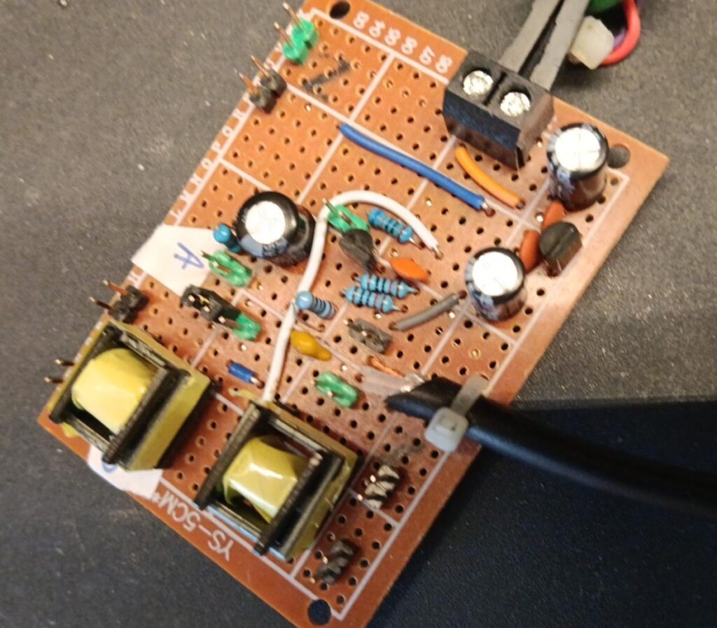
Yesterday I continued the characterization measurements of the fixture I am developing for Bode measurements using an injection transformer.
The work started here:
I then characterized the behavior of the system using a series of purely resistive dividers, trying to understand how strongly the measurement depended on frequency, impedance, and transformer orientation:
The results with resistive loads were very good overall. At this point I wanted to make the test bench progressively more demanding by introducing a reactive component.
In this article I therefore collect the measurements performed with a resistance–capacitive-reactance, once again comparing the two A/B transformer configurations with the result obtained from the LTspice simulation.
Here the behavior became considerably more interesting.
An important note about the trigger
Throughout this measurement campaign I also kept the oscilloscope trigger configuration unchanged.
The trigger is provided through a separate physical 10 kHz line, independently of the frequency of the signal used for the measurement. I chose not to change its configuration during the campaign in order to keep the experimental conditions as constant as possible between different acquisitions.
In the subsequent FFT analyses, a recurring component also appeared around 10 kHz. It is therefore possible that at least part of this component is related to coupling from the trigger line, but I have not yet demonstrated this experimentally.
I preferred not to modify the test bench once the campaign had already started: the influence of the trigger will be checked in a later system configuration.
Test configuration
Before showing the results, it is useful to define precisely the configuration used for this measurement campaign.
The test bench is the same one used in the previous resistive tests, but in this case the branch to ground consists of a capacitor. The upper resistor was kept constant at:
Between the nodes VOUT and VSENSE the secondary of the injection transformer is connected; in the LTspice simulation the injection point is represented by the ideal AC source. The 18 Ω resistor is also present, corresponding to the load permanently installed on the fixture secondary.
The transfer function used in all processing is:
The schematic used in LTspice is shown in the following figure. Wherever possible, the simulation uses the actual measured component values rather than simply their nominal values.
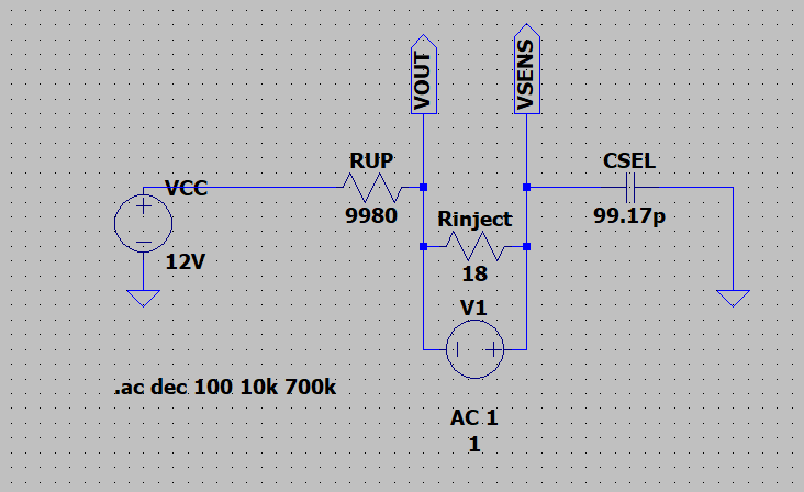
The RUP resistor is 9.980 kΩ, while CSEL is replaced in the different measurement series with the values listed in the table. The injection point is modeled between VOUT and VSENSE, with the 18 Ω resistor present on the fixture secondary.
Capacitors used
Four measurement series were performed while keeping the rest of the test bench unchanged and replacing only capacitor CSEL.
| Nominal value | Measured capacitance | Measured reactance at 50 kHz |
|---|---|---|
| 100 pF | 99.17 pF | -32.1 kΩ |
| 470 pF | 463.5 pF | -6.86 kΩ |
| 2.2 nF | 2.17 nF | -1.47 kΩ |
| 4.4 nF | 4.36 nF | -730.6 Ω |
For an ideal capacitor, the reactance is:
The values listed in the table, however, are those obtained directly from the LCR measurements at 50 kHz.
Frequency range and A/B configurations
For each capacitor, the system was characterized over the range:
Each point was acquired with the two transformer orientations already defined in the previous tests:
- A: transformer terminal A connected to VOUT and terminal B connected to VSENSE;
- B: connections reversed.
The two measurements are processed separately and then combined using the complex geometric mean:
The plots in the following sections therefore show, for each capacitance value, LTspice, measurement A, measurement B, and the A/B mean.
Injection signal amplitude
The amplitude supplied by the generator was not kept constant during the sweep. It was adjusted manually according to frequency and load, increasing VGEN when necessary to keep the acquired signals sufficiently readable.
Throughout the campaign, however, I maintained a maximum limit of 2.5 V, avoiding any further increase in excitation even when one of the two measured signals became very small.
| Frequency | 99.17 pF | 463.5 pF | 2.17 nF | 4.36 nF |
|---|---|---|---|---|
| 10 kHz | 0.3 V | 0.5 V | 0.5 V | 0.5 V |
| 20 kHz | 0.6 V | 0.5 V | 0.5 V | 0.5 V |
| 30 kHz | 0.6 V | 0.5 V | 0.5 V | 0.8 V |
| 50 kHz | 0.7 V | 0.5 V | 0.8 V | 0.8 V |
| 80–120 kHz | 0.7 V | 0.7 V | 1.0 V | 1.0 V |
| 140 kHz | 0.7 V | 0.7 V | 1.5 V | 1.5 V |
| 160–180 kHz | 1.0 V | 1.0 V | 1.5 V | 1.5 V |
| 200 kHz | 1.0 V | 1.0 V | 2.0 V | 1.5 V |
| 220–260 kHz | 1.0 V | 1.0 V | 2.0 V | 2.0 V |
| 280–350 kHz | 1.0 V | 1.5 V | 2.0 V | 2.0 V |
| 370 kHz | 1.0 V | 1.5 V | 2.5 V | 2.0 V |
| 400–450 kHz | 1.3 V | 1.5 V | 2.5 V | 2.0 V |
| 480–700 kHz | 1.6 V | 1.5 V | 2.5 V | 2.0 V |
Data and processing
The waveforms were acquired from the oscilloscope and then processed with the GNU Octave scripts described in the previous articles. Processing includes coherent extraction of the fundamental, magnitude and phase calculation, and acquisition diagnostics.
The raw oscilloscope CSV files are not attached directly to the article because, considering all the acquisitions in the campaign, they require a very large amount of storage.
Instead, I provide in a single ZIP archive the results of the processing performed with Octave, so that the numerical values used to build the plots can be inspected and the observations below can be checked more easily.
Measurements
To verify how the fixture behavior changes when the impedance connected to the injection point becomes reactive, I kept the resistance fixed at 10 kΩ and repeated the measurement with four capacitance values:
100 pF, 470 pF, 2.2 nF, and 4.4 nF.
For each configuration I acquired both transformer orientations, designated A and B and separately processed the magnitude and phase of the VOUT/VSENSE ratio. The plots also show the A/B mean and the comparison with the reference obtained in LTspice.
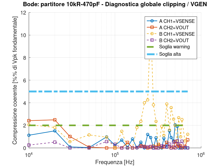
Alongside the Bode plots I also report the diagnostics derived directly from the acquired waveforms, which were used during the campaign to identify conditions in which the signal could become less reliable.
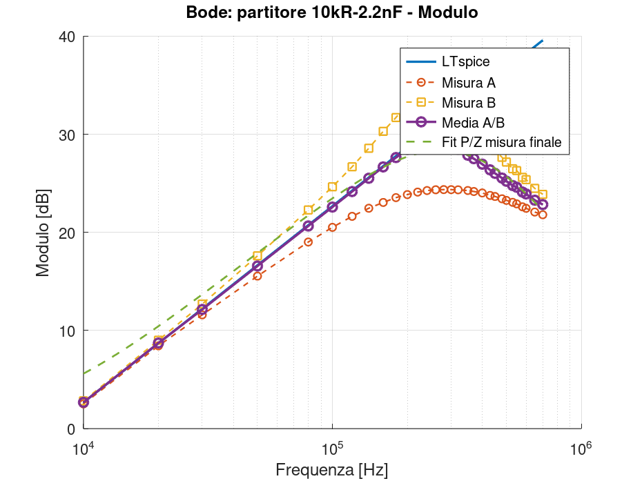
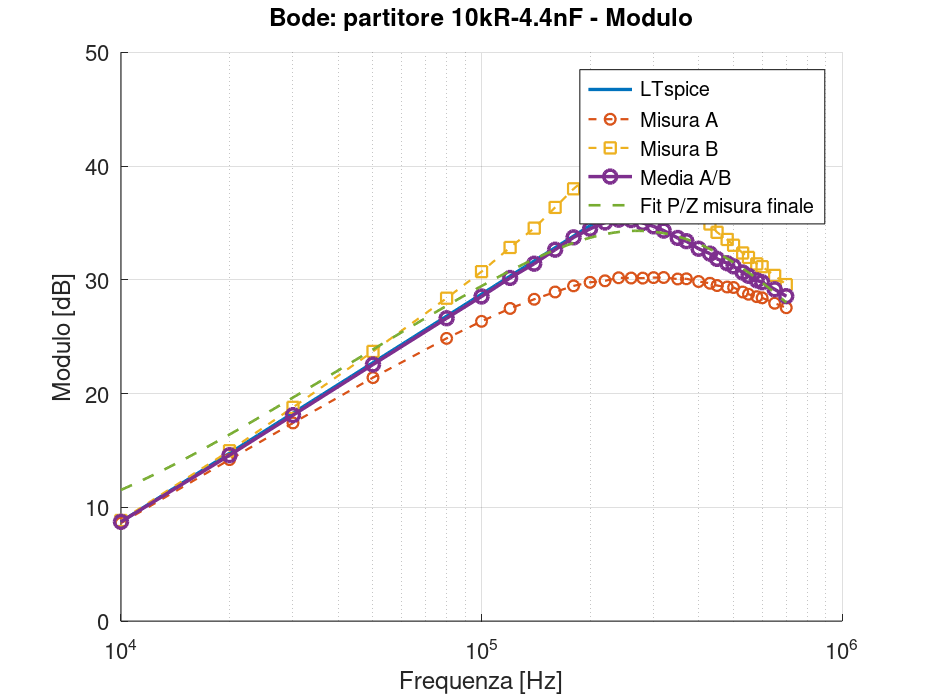
Magnitude – comparison between LTspice and A/B measurements with a reactive load
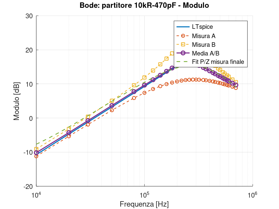
The following four plots show the magnitude of VOUT/VSENSE as a function of frequency. For each capacitance value, the plots show measurements in configurations A and B, their mean, and the response obtained from the LTspice simulation.
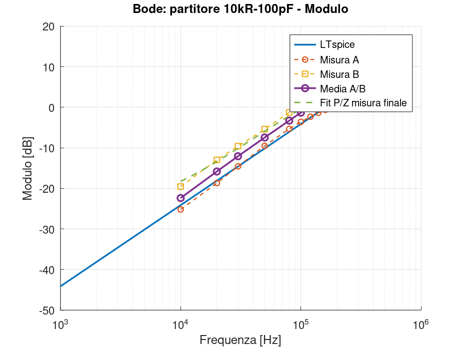 R = 10 kΩ, C = 100 pF. Modulo misurato nelle configurazioni A e B, media A/B e confronto con LTspice.
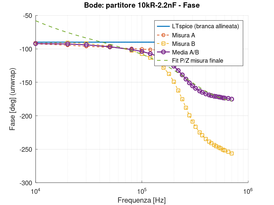
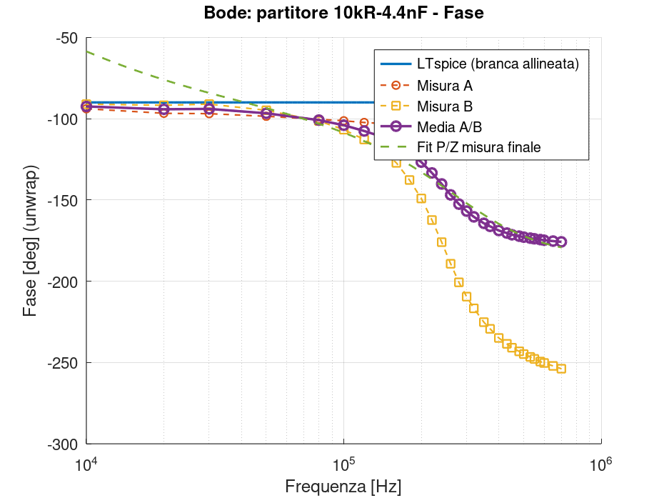
Phase – comparison between LTspice and A/B measurements with a reactive load
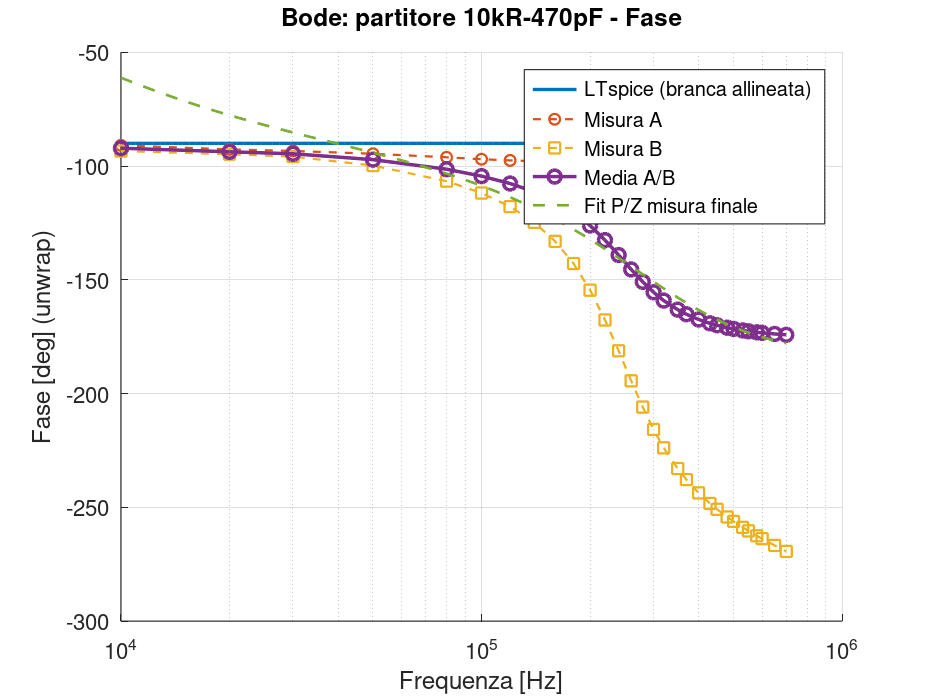
The same four cases are shown here considering the phase of VOUT/VSENSE. The phase is shown continuously using unwrapping, so that the evolution of configurations A and B remains readable even when it exceeds the ±180° display limits.
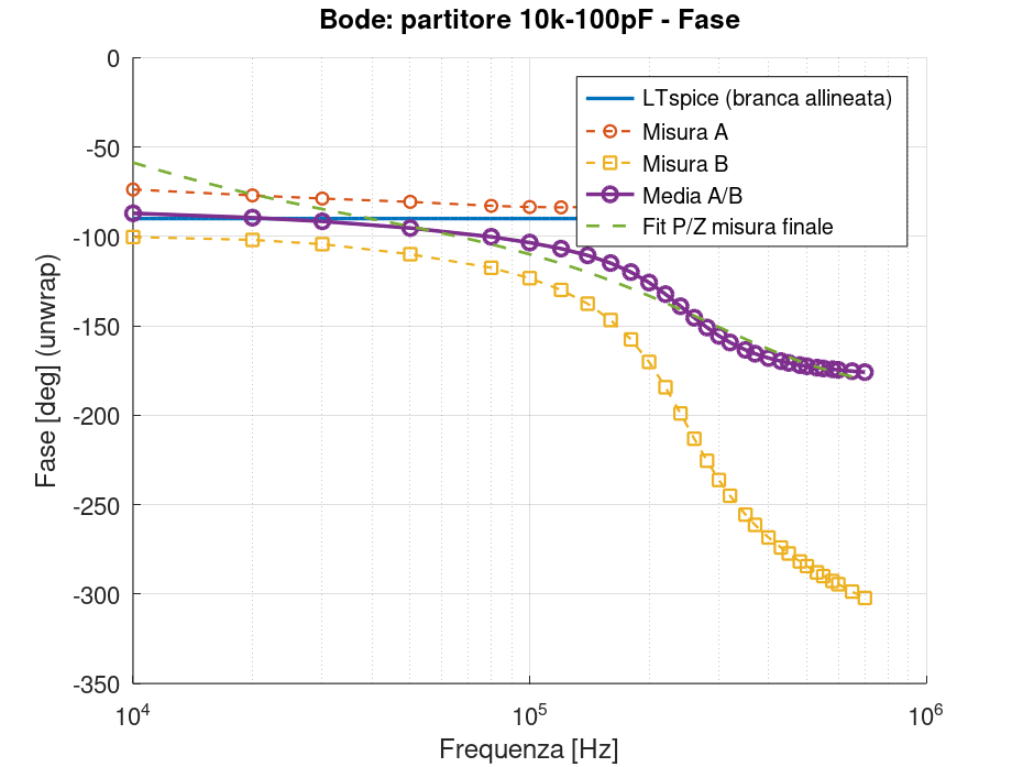 R = 10 kΩ, C = 100 pF. Fase di VOUT/VSENSE: configurazioni A e B, media A/B e riferimento LTspice.
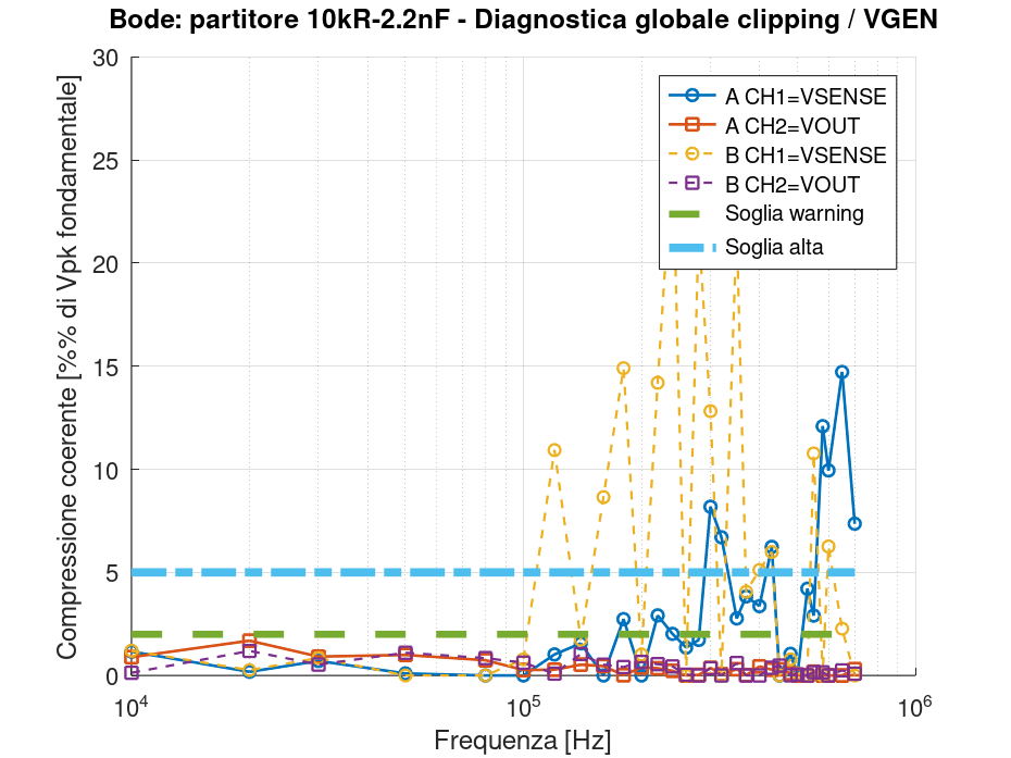
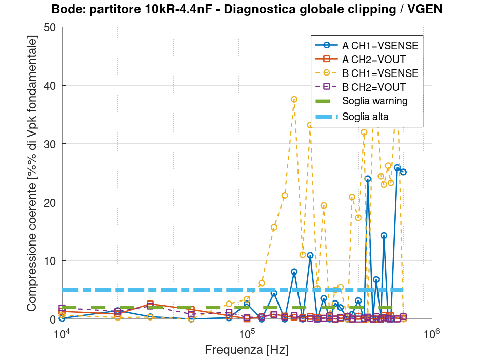
Acquisition diagnostics
During processing I did not use only magnitude and phase. For each acquisition, the script also performs a waveform diagnostic, comparing the reconstructed fundamental with the acquired signal and looking for coherent distortions that may indicate a critical measurement condition.
The plots show the two channels separately in configurations A and B, together with the thresholds used by the script. These results are not automatically interpreted as evidence of clipping: especially when one of the two signals becomes very small, the ratio between the residual and the fundamental can also increase considerably. This point is discussed later in the data analysis.
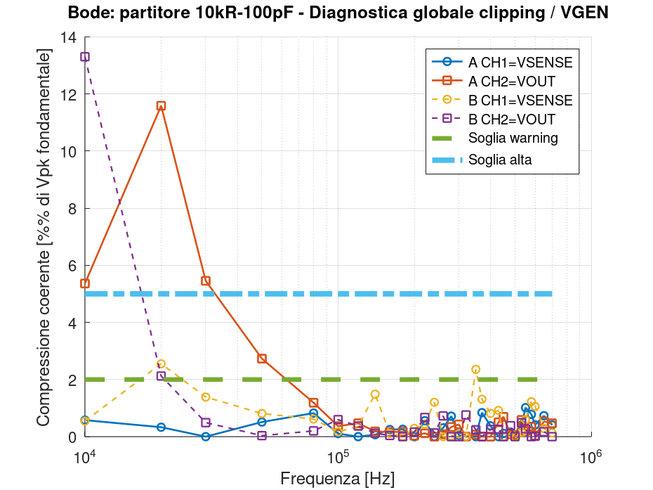 R = 10 kΩ, C = 100 pF. Diagnostica delle quattro acquisizioni A/B utilizzata per controllare la qualità del segnale.
Observations
Before examining the magnitude and phase trends in detail, it is worth focusing on one aspect that emerged during processing of the acquisitions: how effectively the extraction method can recover the fundamental component even when one of the signals becomes very small.
Robustness of the extraction and meaning of the diagnostics
The processing script does not simply derive the magnitude and phase of the ratio between the two channels. For each acquisition it also performs waveform diagnostics, comparing the measured signal with the reconstruction obtained from the harmonic fit and searching for coherent distortions consistent with clipping or compression.
These diagnostics must, however, be interpreted carefully. In reactive-load tests, as frequency increases, one of the two signals can become extremely small. In some acquisitions, the fundamental of the weaker channel falls to around 1 mV peak, while the RMS residual of the fit remains on the order of a few millivolts. Under these conditions the diagnostic index rises rapidly and can exceed the thresholds defined in the script.
This does not necessarily mean that the circuit is actually clipping. When the fundamental becomes very small, even a substantially constant residual represents a very large percentage of the useful signal. The diagnostic should therefore be read primarily as an indication of a progressively more difficult measurement condition, not as automatic evidence of driver saturation or compression.
What is interesting is what happens despite this deterioration. Even at points where the weaker channel becomes comparable to, or even smaller than, the reconstruction residual, the extracted values do not begin to scatter randomly. Magnitude and especially phase continue instead to follow an extremely regular trend consistent with that observed in the series where the signals were much easier to measure.
This behavior provides an important check of the robustness of the coherent fundamental extraction used in the processing. The fit specifically searches for the component at the test frequency and can therefore largely separate it from noise and other non-coherent components in the acquisition.
Of course, this result alone does not demonstrate the absolute accuracy of the measurement. A stable systematic error introduced by the fixture, probes, oscilloscope, or the entire measurement chain can be perfectly repeatable. It does, however, demonstrate something equally important for the rest of the analysis: the regular structures appearing in the plots do not seem to be merely the result of an algorithm losing the signal and beginning to track noise.
Mathematical model of the measurement
To interpret the results obtained with the different test networks systematically, it is useful to introduce a simple mathematical model of the measurement.
The starting point is to distinguish three different elements: the response predicted by the LTspice simulation, the unavoidable differences between the simulated and real circuits, and finally the effect introduced by the fixture and the entire measurement chain.
The transfer function actually measured can therefore be written as:
where HDUT,real represents the actual behavior of the circuit under test, while Efixture collects the effect introduced by the fixture and acquisition chain.
The latter term should not necessarily be interpreted as a simple function of frequency. The measurements show that fixture behavior can also depend on the impedances present on the two sides of the injection point. Therefore, at least at this stage, it is more appropriate to write generically:
Here, the term Z compactly represents the set of impedances with which the fixture interacts. In a more complete description, the impedance seen toward the upstream circuit and that seen toward the downstream circuit from the injection point could be distinguished explicitly.
The real DUT does not necessarily coincide with the model used in LTspice either. We can therefore write:
The term EDUT therefore represents the difference between the ideal or modeled circuit and the physically implemented one: actual component values, tolerances, parasitic capacitances and inductances, wiring, and any other non-ideality not included in the simulation.
Combining the two relationships gives:
This relationship is useful primarily as a conceptual model. It reminds us that a difference between simulation and measurement should not automatically be attributed to the DUT or the transformer: what we observe is the result of the interaction between the real circuit and the measurement system.
Introducing configurations A and B
In my setup the transformer is used in the two orientations A and B. Previous measurements on resistive dividers had already shown that part of the error changes sign—or, more precisely, appears reciprocally—when the transformer orientation is reversed.
It is therefore useful to decompose the fixture contribution into a common component EC and an orientation-dependent component EA.
For configuration A we can write:
while, reversing the transformer:
If the two configurations satisfy this relationship sufficiently well, the complex geometric mean makes it possible to eliminate the orientation-dependent term:
which gives:
The EA component is therefore canceled, while the common component EC remains.
It is precisely this latter term that becomes particularly interesting when the four capacitive-load campaigns are considered together: despite very different capacitance values and progressively more difficult measurement conditions, the residual deviation of the A/B mean from the simulation shows a surprisingly repeatable structure.
There is, however, an important caveat. The previous decomposition implicitly assumes that the DUT contribution and the fixture contribution can be treated as independent factors. This approximation is valid only when the measurement system perturbs the circuit under test negligibly.
In general, however, there is a mutual interaction: the DUT impedances affect fixture behavior and, at the same time, fixture impedances and parasitics alter the circuit being measured. It is therefore useful to introduce conceptually an additional term EDUT,fixture, representing this non-separable component of the error.
Under desirable measurement conditions, EDUT,fixture ≈ 1 is desired, so that, to a first approximation, the DUT and fixture can be regarded as separate contributions. When the impedances of the measurement chain become comparable to those of the DUT, this approximation progressively loses validity.
The 100 pF case is probably the clearest example: the total capacitance introduced by probes, oscilloscope, transformer, wiring, and test bench is no longer negligible compared with the nominal capacitance of the test circuit.
A characteristic frequency recurring across the different measurements
Looking at the magnitude plots of the four capacitive networks together, a very clear common feature appears: the curve obtained from the A/B mean rises with frequency, reaches a maximum, and then begins to decrease.
The position of this maximum changes surprisingly little as the capacitance is varied.
| Nominal capacitance | Measured capacitance | XC measured at 50 kHz | Frequency of the A/B maximum, fmax | Maximum A/B magnitude |
|---|---|---|---|---|
| 100 pF | 99.17 pF | -32.1 kΩ | 260 kHz | 5.992 dB |
| 470 pF | 463.5 pF | -6.86 kΩ | 240 kHz | 16.293 dB |
| 2.2 nF | 2.17 nF | -1.47 kΩ | 260 kHz | 29.331 dB |
| 4.4 nF | 4.36 nF | -730.6 Ω | 240 kHz | 35.291 dB |
The value of 250 kHz that I will use below therefore does not correspond to a single measured point or to a frequency obtained from a fit. It is simply a representative value for the region in which the maxima of the four curves lie.
Since the campaign points are spaced by 20 kHz around the maximum, what the data directly support is therefore that the maximum lies in the 240–260 kHz range. Referring to a characteristic frequency of about 250 kHz is a concise way of expressing this observation without implying a precision that the frequency sampling does not support.
The result becomes even more interesting when compared with the impedances of the four capacitors. The capacitive reactance is:
The LCR measurements at 50 kHz already show that the four DUTs present very different electrical conditions: they range from about -32.1 kΩ for 99.17 pF to about -731 Ω for 4.36 nF.
If, solely to obtain an order of magnitude, we use the measured capacitance values and calculate the reactance at the frequency where each curve reaches its maximum, we obtain:
| Measured capacitance | fmax | XC(fmax) calculated |
|---|---|---|
| 99.17 pF | 260 kHz | ≈ -6.17 kΩ |
| 463.5 pF | 240 kHz | ≈ -1.43 kΩ |
| 2.17 nF | 260 kHz | ≈ -282 Ω |
| 4.36 nF | 240 kHz | ≈ -152 Ω |
These values differ by more than an order of magnitude, while the frequency of the maximum remains confined to the same narrow region.
For the moment, I therefore prefer to limit the conclusion to the experimental observation: the four capacitive networks show a common feature tied to absolute frequency, with a magnitude maximum around 250 kHz, despite the very different impedances presented by the DUT.
This result alone does not yet identify which element of the fixture or measurement chain is responsible. It does, however, rule out at least the simplest interpretation that the phenomenon appears when a single critical capacitor-reactance value is reached.
At this stage I am not attempting to attribute the observed behavior to a specific parasitic element of the fixture or measurement chain. The data show, with good repeatability, a common structure in the same frequency region, but identifying its cause would require a dedicated measurement campaign beyond the scope of this work.
A surprisingly repeatable phase rotation
A second behavior common to all four series concerns phase.
The LTspice simulation of the network used as the DUT predicts, over the frequency range considered, a phase essentially equal to −90°. The measurements instead show a progressive rotation that is already clearly visible in the region roughly between 80 and 100 kHz and then increases with frequency.
The most interesting aspect, however, is not merely the existence of this deviation, but its extraordinary repeatability as the capacitance is varied.
The following table reports, for several significant frequencies, the difference between the phase of the A/B mean and that predicted by LTspice.
| Frequency | 99.17 pF | 463.5 pF | 2.17 nF | 4.36 nF |
|---|---|---|---|---|
| 100 kHz | -13.45° | -14.40° | -13.92° | -14.03° |
| 200 kHz | -35.78° | -36.12° | -35.87° | -36.73° |
| 300 kHz | -65.60° | -65.46° | -65.30° | -66.86° |
| 500 kHz | -82.59° | -81.55° | -81.18° | -82.87° |
| 700 kHz | -85.91° | -84.15° | -85.15° | -85.77° |
The quantity reported in the table is defined as:
The similarity is remarkable. At 200 kHz, for example, four DUTs with capacitances ranging from about 100 pF to 4.4 nF produce a deviation confined to approximately −35.8° to −36.7°. The trend remains substantially the same at higher frequencies.
This result is even more significant considering that, in the series with larger capacitances, some acquisitions are made with one of the two signals extremely small and therefore under much less favorable signal-to-noise conditions. Despite this, the extracted phase continues to follow the same evolution observed in the easier measurements.
It therefore does not seem plausible to interpret this structure as simple random scatter caused by measurement difficulty.
At the same time, the same behavior had not appeared in the previous tests on purely resistive dividers. This detail is important: it prevents the observed deviation from being described simply as a DUT-independent fixture transfer function.
The results instead seem to indicate an extremely repeatable contribution arising from the interaction between the fixture and a DUT with reactive impedance.
Using the model introduced above, this contribution can conceptually be associated with the term:
For the moment I am not attempting to identify which physical mechanism produces this rotation. Determining whether transformer parasitic capacitance, probes, wiring, perfboard geometry, or a combination of several effects dominates would require tests specifically designed to separate them.
The experimental result of interest here is simpler: introducing a capacitive component into the DUT produces a phase rotation that is strongly frequency-dependent but surprisingly weakly dependent on the capacitance value, whereas the same phenomenon was not evident in the previous purely resistive tests.
So what? How professional instrumentation addresses the problem
At this point the natural question is: if measurement with an injection transformer can become so sensitive to the impedances on the two sides of the injection point, how is this problem addressed in professional instruments?
Rohde & Schwarz documentation is very explicit. To obtain a loop-gain measurement representative of the actual loop, the injection point must be located where there is a single loop path and, above all, the impedance seen in the feedback direction must be much greater than that seen backward toward the converter output. In a typical power supply, the output impedance can be on the order of milliohms, while the divider and compensation network can have impedances on the order of kΩ.
Rohde & Schwarz also uses an injection resistor of only 5 Ω, intentionally negligible compared with the impedances of the feedback network.
The same guidance appears in Picotest documentation: for a correct measurement, one side of the injection point must have an impedance much greater than the other. Picotest specifically identifies the sense divider of a power supply as a favorable point because the power-supply output impedance is very low compared with that of the feedback network.
This is very different from the test bench I deliberately used in these tests.
In my case, looking at the two sides of the injection point in AC, one side presents:
while on the other side we essentially have the capacitor reactance:
and therefore an impedance that decreases as frequency increases.
Already from the measurements made at 50 kHz:
| Nominal capacitance | Measured capacitance | |XC| at 50 kHz |
|---|---|---|
| 100pF | 99.17pF | 32.1 kΩ |
| 470pF | 463.5pF | 6.86 kΩ |
| 2.2nF | 2.17nF | 1.47 kΩ |
| 4.4nF | 4.36nF | 730.6 Ω |
These are the values measured with the LCR meter.
Around the 250 kHz region identified in the plots, these values become approximately:
| Nominal capacitance | Measured capacitance | |XC| at 250 kHz |
|---|---|---|
| 100pF | 99.17pF | ≈ 6.42 kΩ |
| 470pF | 463.5pF | ≈ 1.37 kΩ |
| 2.2nF | 2.17nF | ≈ 294 Ω |
| 4.4nF | 4.36nF | ≈ 146 Ω |
Thus, as frequency increases, the test bench moves progressively farther from the typical condition recommended for a real loop-gain measurement: on one side there remain about 10 kΩ, while on the other the capacitive impedance becomes progressively lower.
There is, however, an important distinction here: this fact alone does not explain the turnover observed in the plots. The frequency dependence of XC is already present in the LTspice simulation and, in the ideal circuit, produces the expected trend of the ratio. It therefore cannot directly be the cause of the difference between LTspice and measurement.
It can instead explain why, as frequency increases, the test bench becomes progressively more sensitive to fixture non-idealities: parasitic capacitances, probe impedances, coupling, and other elements absent from the ideal LTspice model become increasingly important when they interact with such unbalanced impedances.
This also makes the purpose of the tests easier to understand. I am not reproducing the optimum condition in which an injection transformer is normally used; I am deliberately placing the fixture in an unfavorable condition to observe its behavior.
Another interesting point comes from OMICRON Lab: even a professional transformer such as the B-WIT 100 is not an ideal component. OMICRON specifies, for example, a typical primary-to-secondary capacitance of about 120 pF. This is an important reminder: professional techniques do not work because the transformer is free of parasitics, but because the transformer, injection point, terminations, and probing are chosen so that these effects are sufficiently small relative to the circuit being measured. Picotest also emphasizes that the effectively usable bandwidth of an injection transformer depends strongly on termination and interconnection with the DUT.
For now, therefore, I am not looking for a universal fixture correction. The results of this campaign instead suggest that the first requirement for a good measurement is to choose an injection point where the fixture perturbs the real circuit as little as possible.
Sources:
- Rohde & Schwarz – Power supply control loop response measurements
- Picotest – J2110A Solid State Injector
- Picotest – J2100A Injection Transformer
- OMICRON Lab – Injection Transformers B-WIT/B-LFT
Conclusions from this first phase
At this point the overall picture is fairly clear.
When measuring the loop gain of a power supply, the injection point is normally chosen between the output and the feedback network. Ideally this provides a very favorable condition: looking toward the power-supply output, one sees a low impedance, while looking toward the feedback network one normally sees a significantly higher impedance, often set by resistances on the order of a few kΩ.
The condition sought is therefore, qualitatively:
The test bench used in this campaign was deliberately moved far away from this condition.
In my case, one side of the injection point had a resistance of about 10 kΩ, while the other side had a capacitive impedance that progressively decreases as frequency increases. This is therefore not the typical condition in which I expect to use the fixture in practice.
This was intentional, however. The purpose of these tests was not only to verify that the transformer worked under the most favorable conditions, but also to understand how far it was possible to move away from them and, above all, whether a sufficiently general relationship could be identified to compensate fixture behavior even under very different impedance conditions.
For the moment, the answer I obtain from the data is:
The measurements show extremely regular and repeatable behavior, but they also show that the fixture and the circuit under test can interact non-negligibly when impedance conditions become unfavorable. In these situations, characterizing the transformer as a simple DUT-independent transfer function and then applying a universal correction does not appear sufficient.
This does not mean that a more complete characterization is impossible. It only means that, with the data collected so far, I do not have sufficient evidence to define a general relationship that I consider reliable. Further measurements in this direction can be performed later, possibly with a more automated acquisition system.
To proceed toward the practical goal of the project, I will therefore take a different approach: I will use the fixture under the conditions for which this technique is normally employed, choosing injection points with a large difference between the impedances seen in the two directions.
The first step will be to return to the small board with the LM358 TI that I used in the initial tests. Those measurements had already shown good agreement with LTspice, but I can now repeat them with much greater knowledge of the fixture’s behavior and limitations.
I am also waiting for additional TI LM358 devices, ordered specifically to build new test DUTs with a structure more similar to that of a real feedback circuit. I also want to preserve the LTspice comparison in these experiments by using the same component and, as far as possible, controlled conditions.
The next step will finally be the one for which this fixture was built:
to measure the loop gain of a hybrid power supply that I designed and built before I started keeping this public lab log.
I have not yet discussed that power supply on the blog precisely because the project predates this lab log. When I reach the Bode measurements, it will therefore also be an opportunity to present it, describe how it works, and finally compare the response predicted by simulation with that measured on the real circuit.
Appendix – Spectral verification of the FFT acquisitions
In the appendix I also include a spectral verification of the acquisitions used to derive the Bode plots of the capacitive test bench.
The purpose of this analysis is not to add another level of DUT modeling, but to check the quality of the measurement setup and determine whether, in addition to the fundamental, spurious components, harmonics, or recurring signatures attributable to the acquisition chain appear.
The FFTs were calculated from the oscilloscope CSV files using a GNU Octave script developed specifically for this work.
For each test-bench configuration, the spectra of acquisitions A and B are summarized to highlight both components coherent with the applied signal and any residual contributions common to the instrumentation.
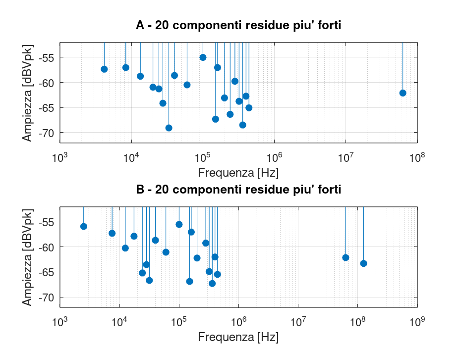
The following four figures show the FFT summary for the configurations 10 kΩ + 100 pF, 10 kΩ + 470 pF, 10 kΩ + 2.2 nF and 10 kΩ + 4.4 nF.
In all cases, the analysis confirms that the fundamental is isolated correctly and that the observed residual components are largely weak, scattered, or attributable to expected harmonics and the spectral signature of the acquisition system.
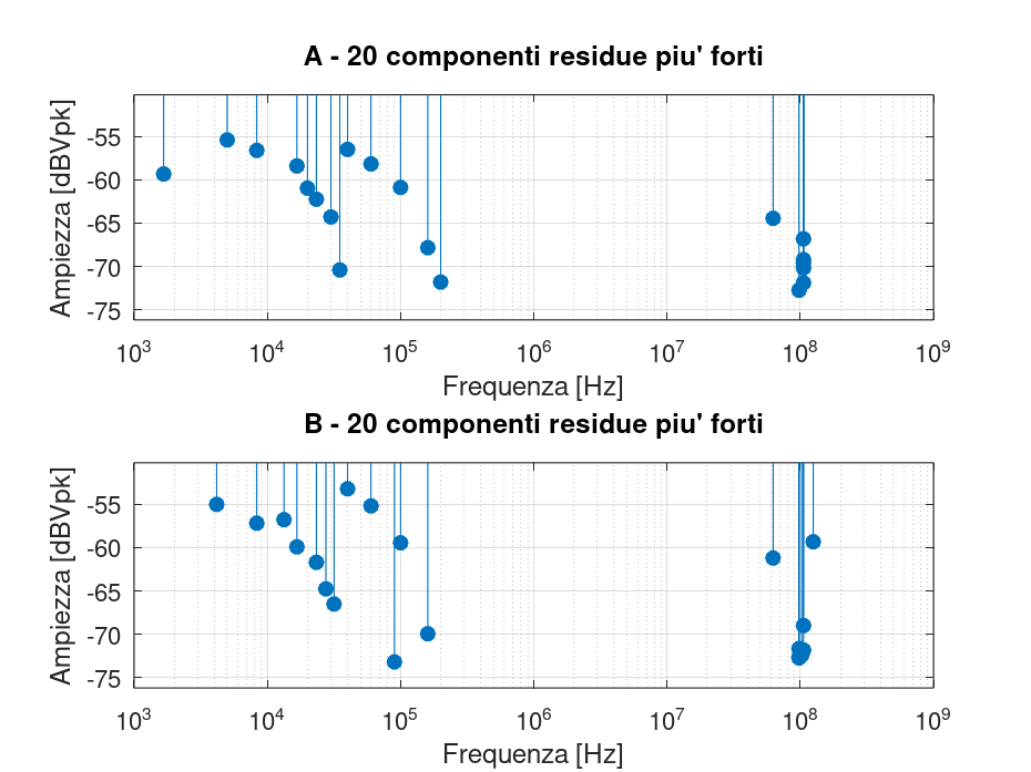 Banco 10 kΩ + 100 pF. Anche nel caso più critico, in cui la capacità nominale è molto piccola e le capacità parassite della fixture e delle sonde diventano relativamente più importanti, lo spettro residuo resta leggibile e coerente. Le componenti spurie osservate sono deboli e non suggeriscono instabilità o inquinamenti anomali del setup.
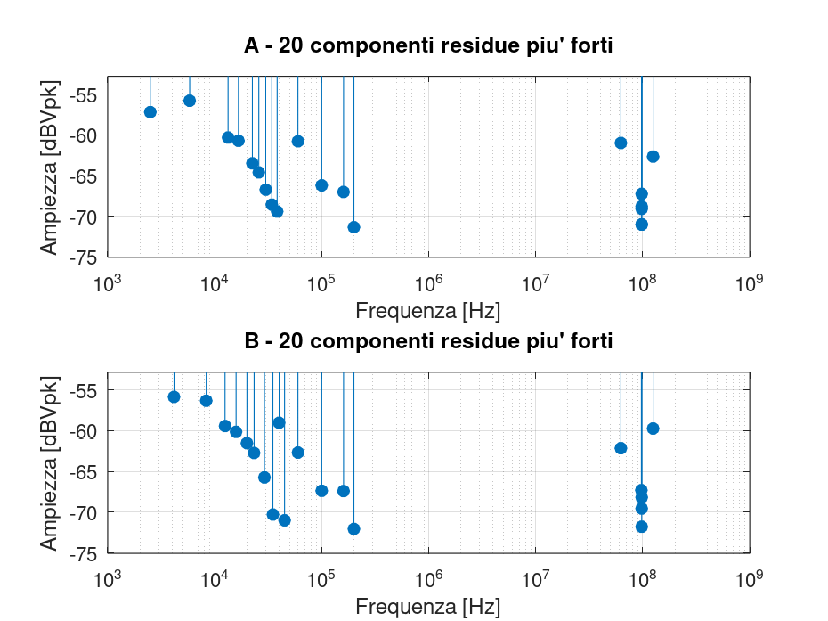
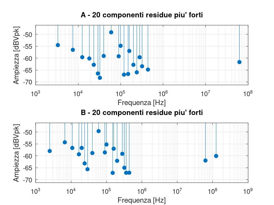
Overall, this appendix increases confidence in the quality of the measurements presented in the main body of the article.
The FFTs show that:
- the fundamental is extracted correctly;
- the expected harmonics, when present, appear consistently with the applied signal;
- the other residual components are generally weak and scattered;
- there also plausibly appears to be a spectral signature of the acquisition system, most likely related to the oscilloscope and its ADC chain, but not to an extent that compromises interpretation of the Bode plots.
For this reason, I regard this analysis not as a secondary result, but as an important verification of the experimental quality of the setup: if I have managed to reveal primarily the spectral signature of the instrumentation, it means that the test bench and measurement procedure are operating under generally clean conditions.